Semiconductor on insulator structure comprising a plasma nitride layer and method of manufacture thereof

a technology of semiconductor on insulator and plasma nitride, which is applied in the direction of semiconductor devices, basic electric elements, electrical equipment, etc., can solve the problems of wasting one of the substrates, not having suitable thickness uniformity, and time-consuming and costly methods

Active Publication Date: 2019-02-28
GLOBALWAFERS CO LTD
View PDF0 Cites 202 Cited by
  • Summary
  • Abstract
  • Description
  • Claims
  • Application Information

AI Technical Summary

Problems solved by technology

This method is time-consuming and costly, wastes one of the substrates and generally does not have suitable thickness uniformity for layers thinner than a few microns.
Concurrently with the heating or annealing of the bonded wafer, the particles earlier implanted in the donor wafer weaken the cleave plane.
Exposure to the elevated temperature causes initiation and propagation of cracks along the cleave plane, thus separating a portion of the donor wafer.
The crack forms due to the formation of voids from the implanted ions, which grow by Ostwald ripening.
The pressurized gases in the platelets propagate micro-cavities and micro-cracks, which weaken the silicon on the implant plane.
However, if the thermal treatment is continued for a longer duration and / or at a higher temperature, the micro-crack propagation reaches the level where all cracks merge along the cleave plane, thus separating a portion of the donor wafer.
Common solutions to this include CMP, which is costly and may leave scratches or thickness variation.

Method used


Image

  • Semiconductor on insulator structure comprising a plasma nitride layer and method of manufacture thereof
  • Semiconductor on insulator structure comprising a plasma nitride layer and method of manufacture thereof
  • Semiconductor on insulator structure comprising a plasma nitride layer and method of manufacture thereof

Examples


Embodiment Construction

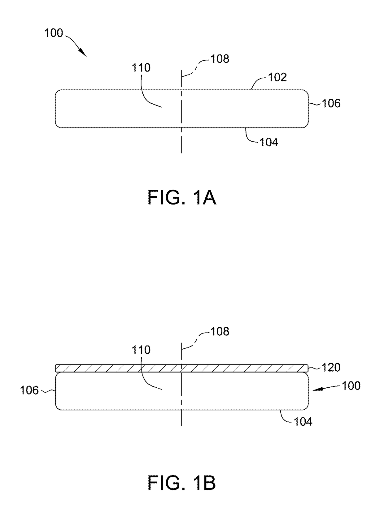
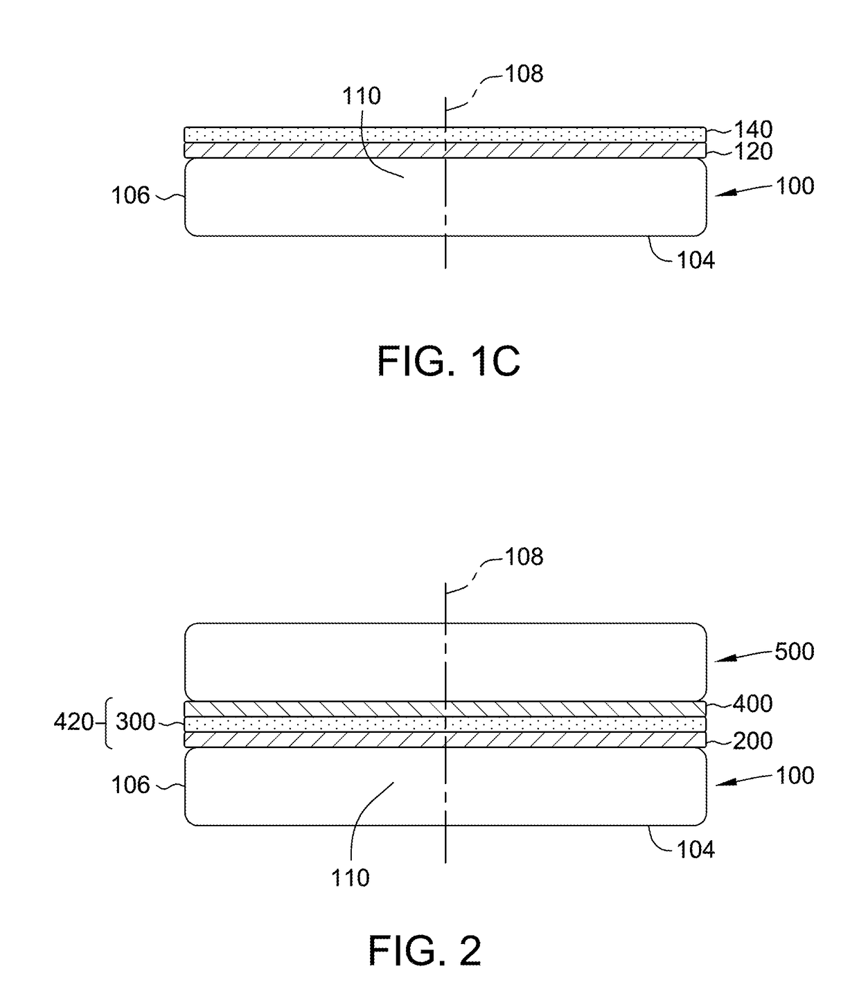
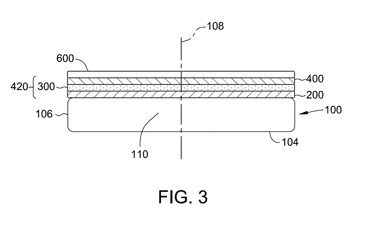
[0021]The present invention is directed to a multi-layered semiconductor-on-insulator structure (SOI, e.g., a silicon-on-insulator structure) that resists impurities contained in a handle substrate from having an influence on the device. The dielectric layer in the semiconductor-on-insulator structure may comprise one or more insulating layers located between the handle substrate and the donor substrate or device layer. The one or more insulating layers in the SOI structure according to the present invention may include silicon nitride, silicon oxide, silicon oxynitride, and combinations of these materials. Preferably, the dielectric layer comprises a multilayer comprising at least two insulating layers comprising these materials, or at least three insulating layers, or more insulating layers. According to some embodiments of the present invention, the insulating layer may comprises an oxide-nitride-oxide dielectric (ONO) in which an oxide layer in interfacial contact with the handl...


PUM

PropertyMeasurementUnit
molar ratioaaaaaaaaaa
thicknessaaaaaaaaaa

Abstract

A method is provided for preparing a semiconductor-on-insulator structure comprising a silicon nitride layer deposited by plasma deposition.

Description

CROSS REFERENCE TO RELATED APPLICATION(S)[0001]This application claims the benefit of priority to U.S. provisional application Ser. No. 62 / 304,381, which was filed Mar. 7, 2016, the disclosure of which is hereby incorporated by reference as if set forth in its entirety.FIELD OF THE INVENTION[0002]The present invention generally relates to the field of semiconductor wafer manufacture. More specifically, the present invention relates to a method of a semiconductor-on-insulator (e.g., silicon-on-insulator) structure.BACKGROUND OF THE INVENTION[0003]Semiconductor wafers are generally prepared from a single crystal ingot (e.g., a silicon ingot) which is trimmed and ground to have one or more flats or notches for proper orientation of the wafer in subsequent procedures. The ingot is then sliced into individual wafers. While reference will be made herein to semiconductor wafers constructed from silicon, other materials may be used to prepare semiconductor wafers, such as germanium, silicon...

Claims


Application Information

Patent Timeline
Patent Type & Authority Applications(United States)
IPC IPC(8): H01L21/762H01L21/02H01L27/12
CPCH01L21/76254H01L21/02274H01L21/0262H01L27/1203H01L21/0214
Inventor KWESKIN, SASHA JOSEPH
Owner GLOBALWAFERS CO LTD
Why Eureka
Try Eureka