Thin film transistor substrate and display device

Active Publication Date: 2019-02-28
HANNSTAR DISPLAY CORPORATION
View PDF0 Cites 9 Cited by
  • Summary
  • Abstract
  • Description
  • Claims
  • Application Information

AI Technical Summary

Benefits of technology

[0007]In the film structure in the electrostatic protection area of the display device of the present invention, since the sealant replaces the insulating material with a high dielectric constant (high-K material) included in the electronic components in the display region or the peripheral region, the dielectric constant of the surrounding of the display device is decreased to reduce the storage of electrostatic charges, so as to restrain the occurrence of electrostatic discharge or decrease the damaging influence damage to the display device caused by electrostatic discharge. Furthermore, because th

Problems solved by technology

The display device inevitably stores electrostatic charges in its interior, and therefore electrostatic discharge easily occurs.
Since this phenomenon is usually accompanied by a large amount of electrostatic charge, the static-sensitive componen

Method used


Image

  • Thin film transistor substrate and display device
  • Thin film transistor substrate and display device
  • Thin film transistor substrate and display device

Examples


Embodiment Construction

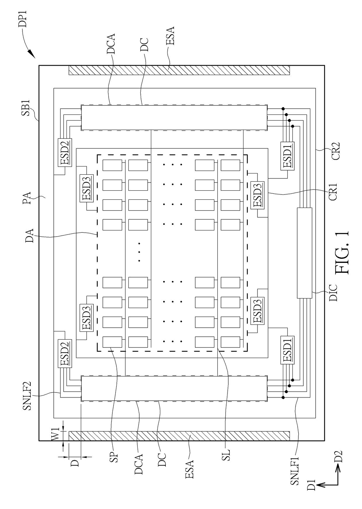
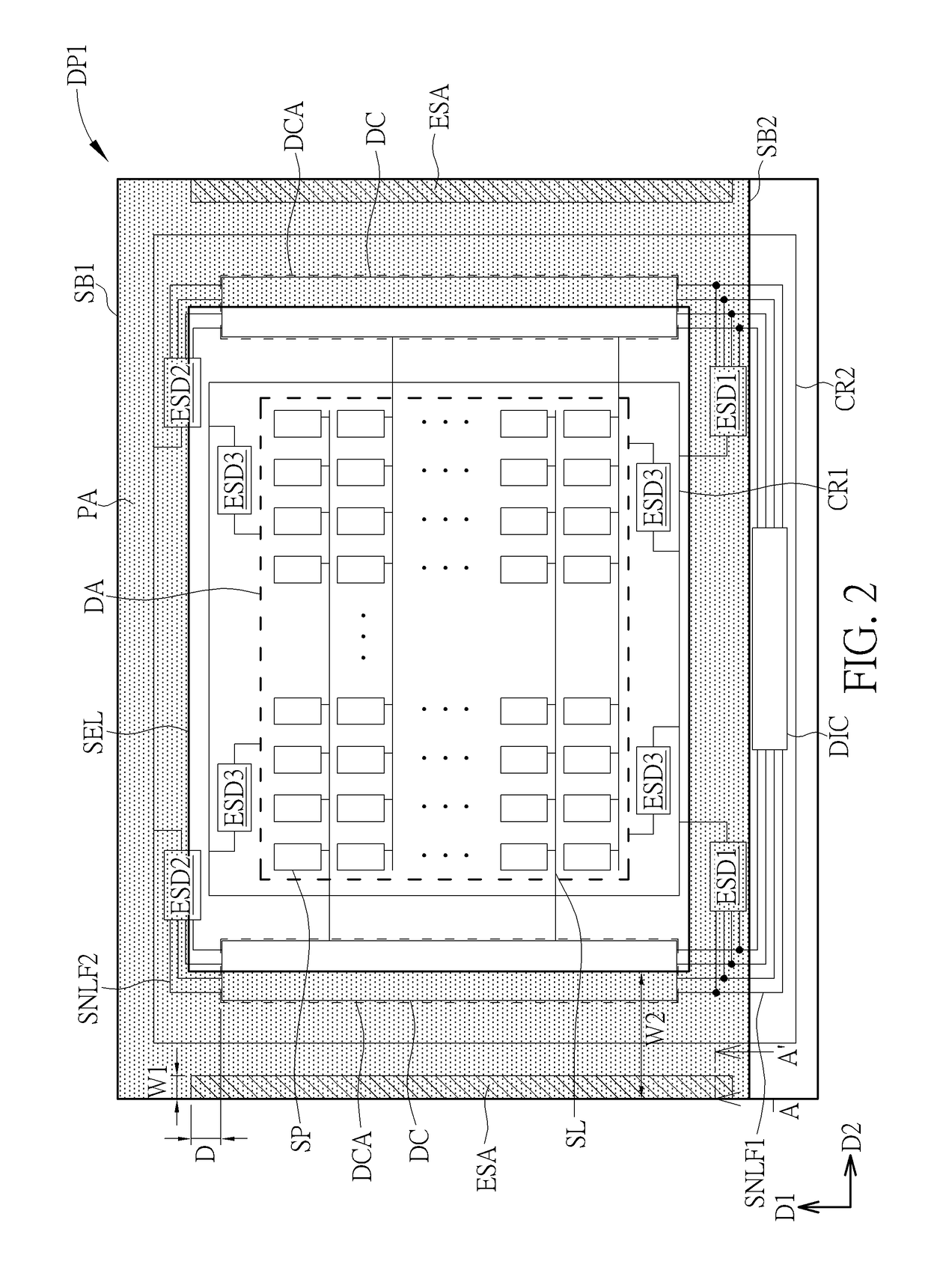
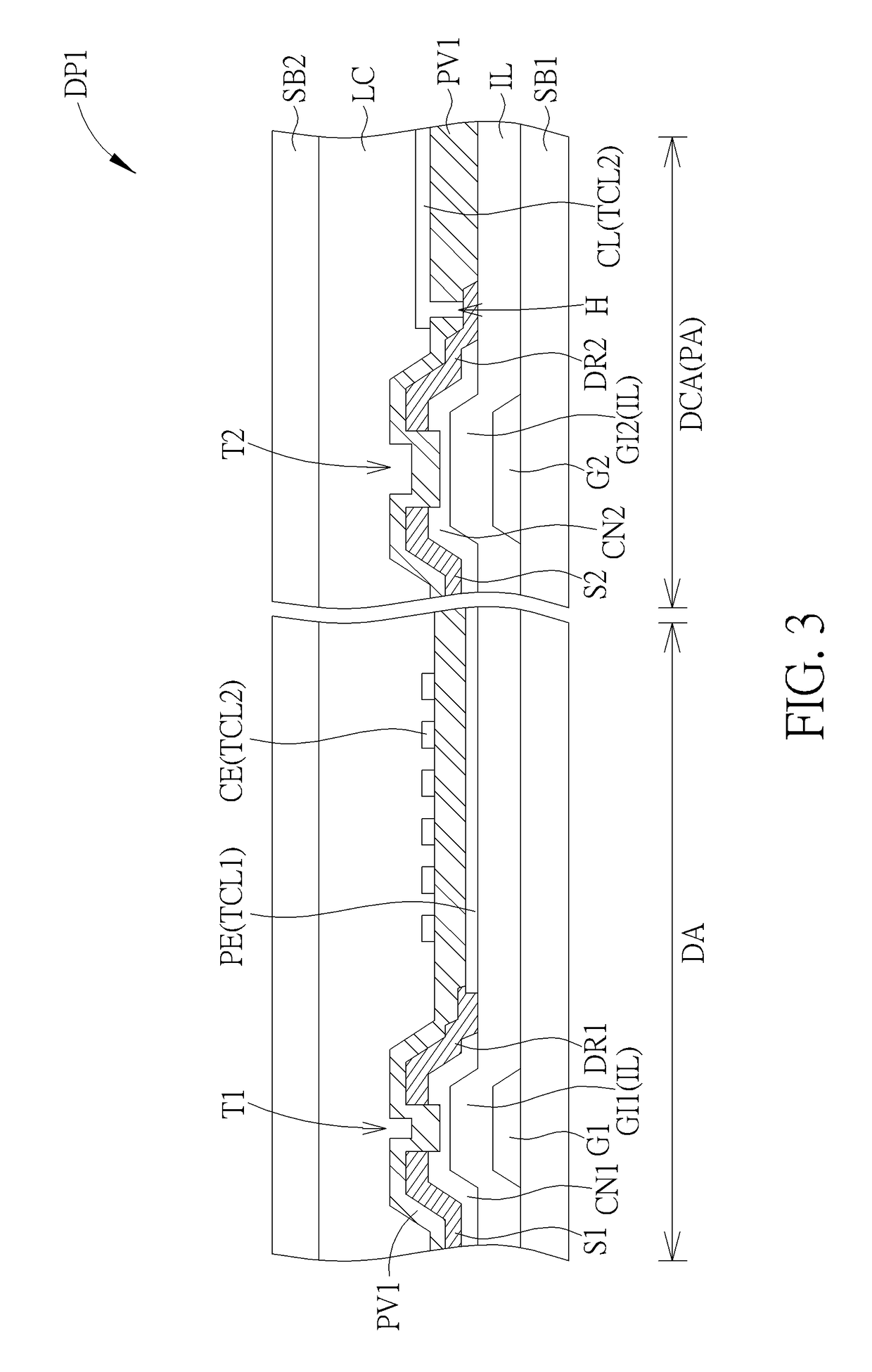
[0018]To provide a better understanding of the present invention to those skilled in the technology, preferred embodiments will be detailed as follows. The preferred embodiments of the present invention are illustrated in the accompanying drawings with numbered elements to elaborate on the contents and effects to be achieved. It should be noted that the drawings are simplified schematics, and therefore show only the components and combinations associated with the present invention, so as to provide a clearer description of the basic architecture or method of implementation. The components would be complex in reality. In addition, for ease of explanation, the components shown in the drawings may not represent their actual number, shape, and dimensions; details can be adjusted according to design requirements.

[0019]FIG. 1 and FIG. 2 are schematic diagrams showing a top view of a display device of a first embodiment of the present invention, wherein FIG. 1 shows a thin film transistor ...


PUM


Abstract

A thin film transistor substrate having a display region and a peripheral region, and the thin film transistor substrate includes a first substrate, scan lines, data lines, an insulating layer, first thin film transistors, at least one passivation layer and at least one gate driving circuit. The first substrate has an electrostatic protection area and a driving circuit area, and the electrostatic protection area and the driving circuit area are situated in the peripheral region. The scan lines, the data lines and the first thin film transistors are disposed in the display region. The insulating layer includes a gate insulator of the first thin film transistor, and the passivation layer is disposed on the insulating layer. The gate driving circuit is disposed in the driving circuit area. At least one of the passivation layer and the insulating layer are not disposed in the electrostatic protection area.

Description

BACKGROUND OF THE INVENTION1. Field of the Invention[0001]The present invention relates to a thin film transistor substrate and a display device, and more particularly to a thin film transistor substrate and a display device that can mitigate the damaging effects of electrostatic discharge and decrease water vapor invasion.2. Description of the Prior Art[0002]A conventional display device is composed of two substrates and layers with various electronic components disposed between the substrates to display images. Since such a display device has the characteristics of thin appearance, low power consumption and no radiation pollution, it has been widely used in many kinds of portable or wearable electronic products, such as notebooks, smart phones, watches, and display devices in cars, for transmitting and displaying information more conveniently.[0003]The display device inevitably stores electrostatic charges in its interior, and therefore electrostatic discharge easily occurs. In so...

Claims


Application Information

Patent Timeline
IPC IPC(8): H01L23/60H02H7/20H01L27/12H02H9/04
CPCH01L23/60H02H7/20H01L27/124H02H9/041H01L27/1214H01L27/1248H01L27/0292H01L27/0296G02F1/136204
Inventor LIN, SUNG-CHUNHU, HSIEN-TANGLIU, HSUAN-CHENCHAN, CHIEN-TING
Owner HANNSTAR DISPLAY CORPORATION
Why Eureka
Try Eureka