Digital alloy based back barrier for p-channel nitride transistors

a digital alloy and back barrier technology, applied in the field of iiinitride transistors, can solve the problems that thick analog algan with high al content cannot be grown on gan buffers, and the fundamental limit of using analog algan alloys

Active Publication Date: 2019-02-28
HRL LAB
View PDF9 Cites 2 Cited by
  • Summary
  • Abstract
  • Description
  • Claims
  • Application Information

AI Technical Summary

Benefits of technology

[0028]Certain embodiments may provide various technical advantages depending on the implementation. For example, a technical advantage of some embodiments may incl

Problems solved by technology

However thick analog AlGaN with high Al content cannot be grown on GaN buffer due to the la

Method used


Image

  • Digital alloy based back barrier for p-channel nitride transistors
  • Digital alloy based back barrier for p-channel nitride transistors
  • Digital alloy based back barrier for p-channel nitride transistors

Examples


Embodiment Construction

[0043]It should be understood at the outset that, although example embodiments are illustrated below, the present technology may be implemented using any number of techniques, whether currently known or not. The present technology should in no way be limited to the example implementations, drawings, and techniques illustrated below. Additionally, the drawings are not necessarily drawn to scale.

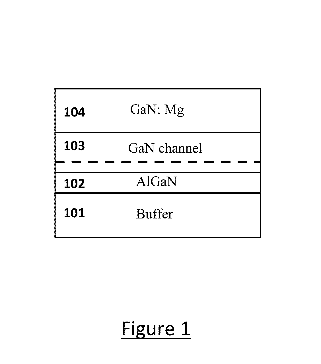
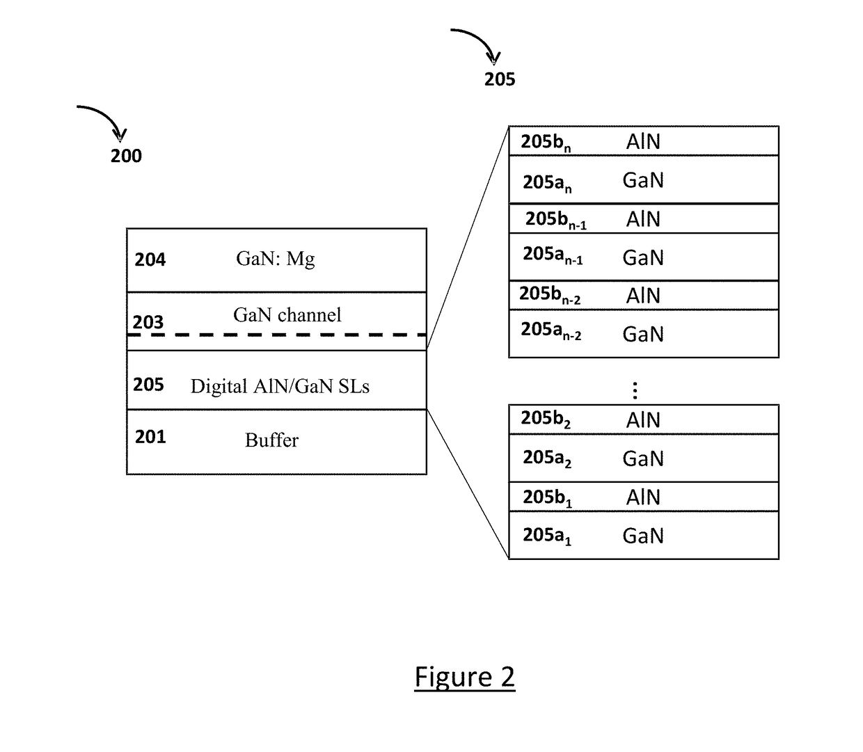
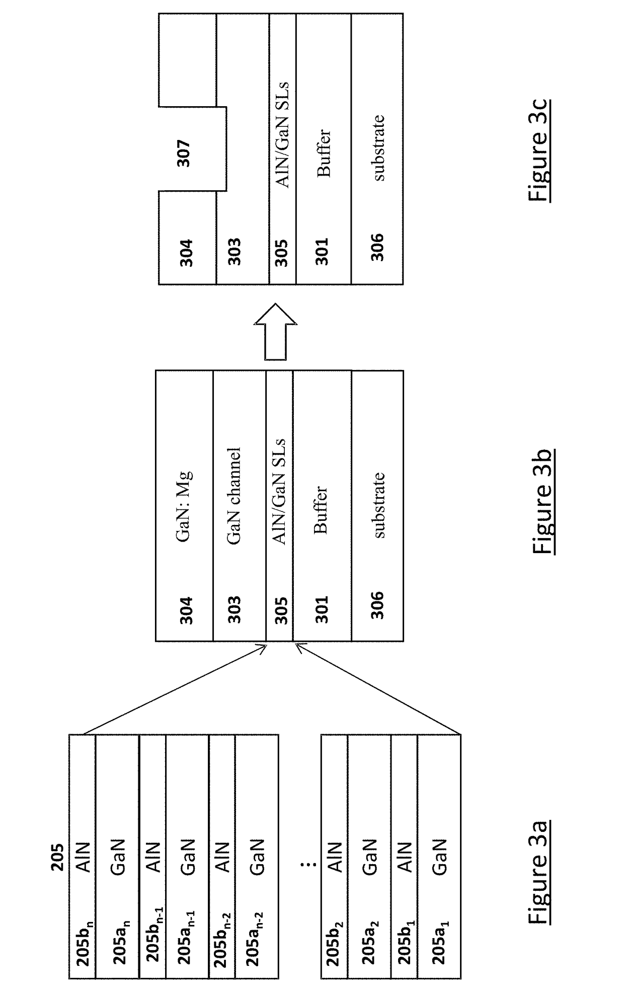
[0044]Recently, GaN transistors have revolutionized high power and high speed switching electronics and there is a constant push, driven by the application demands, for higher and higher power handling capacities. GaN transistor's power handling capacity depends directly on the channel conductivity.

[0045]III-Nitride semiconductor materials (Aluminum, Indium, Gallium)Nitride are excellent wide band gap semiconductors very suitable for modern electronic and optoelectronic applications. Though this disclosure describes the technology using GaN, the proposed technology applies to any of the III-Ni...


PUM


Abstract

A III-nitride power handling device and the process of making the III-nitride power handling device are disclosed that use digital alloys as back barrier layer to mitigate the strain due to lattice mismatch between the channel layer and the back barrier layer and to provide increased channel conductivity. An embodiment discloses a GaN transistor using a superlattice binary digital alloy as back barrier comprising alternative layers of AlN and GaN. Other embodiments include using superlattice structures with layers of GaN and AlGaN as well as structures using AlGaN/AlGaN stackups that have different Aluminum concentrations. The disclosed device has substantially increased channel conductivity compared to traditional analog alloy back barrier devices.

Description

TECHNICAL FIELD[0001]The present disclosure is directed in general to the area of III-Nitride transistors and in particular to the design and fabrication of P-Channel GaN Transistors.BACKGROUND OF THE DISCLOSURE[0002]GaN power integrated circuits (IC) have the potential of dramatically reducing the size and weight of power electronic systems, thereby substantially reducing the cost of power electronic devices. P-channel GaN-transistor is a critical component for making GaN power ICs. Such power electronic systems are widely needed in electric / hybrid vehicles, more-electric aircrafts, as well as many consumer electronic products.[0003]A variety of GaN transistors are known and they include P-Channel transistors in conjunction with N-Channel transistors using an analog alloy to improve conductivity. The use of a tertiary alloy such as AlGaN (Aluminum-Gallium-Nitride) is often referred to as analog alloy in the art. To increase power handling capacity of GaN transistors, several techni...

Claims


Application Information

Patent Timeline
IPC IPC(8): H01L29/778H01L29/15H01L29/20H01L29/205H01L29/207H01L29/66
CPCH01L29/7785H01L29/155H01L29/66462H01L29/205H01L29/207H01L29/2003H01L29/4236H01L29/7781
Inventor CHU, RONGMINGCAO, YU
Owner HRL LAB
Why Eureka
Try Eureka