Mounting substrate, waveguide module, integrated circuit-mounted substrate, microwave module

Active Publication Date: 2019-02-28
NIDEC CORP +1
View PDF2 Cites 16 Cited by
  • Summary
  • Abstract
  • Description
  • Claims
  • Application Information

AI Technical Summary

Benefits of technology

[0014]According to an exemplary embodiment the present disclosure, it is possible to reduc

Problems solved by technology

Conversely, at lower frequencies, the structure requires large size, and the direction of waveguiding is restricted.
Thus, the first structure has a problem in that the processing circuitry which is constituted by the microwave IC and the mounting substrate thereof becomes large in size.
In certain example experiments, an MSL is said to suffer about

Method used


Image

  • Mounting substrate, waveguide module, integrated circuit-mounted substrate, microwave module
  • Mounting substrate, waveguide module, integrated circuit-mounted substrate, microwave module
  • Mounting substrate, waveguide module, integrated circuit-mounted substrate, microwave module

Examples


Example

Application Example 1

[0192]Hereinafter, constructions for applying the microwave module 1000 to radar devices will be described. Specifically, examples of radar devices in which the microwave module 1000 and radiating elements are combined will be described.

[0193]First, the construction of a slot array antenna will be described. Although the slot array antenna is illustrated as having horns, one may choose to provide or not provide any horns.

[0194]FIG. 24 is a perspective view schematically showing a partial structure of a slot array antenna 300 having a plurality of slots functioning as radiating elements. The slot array antenna 300 includes: a first conductive member 310 having a plurality of slots 312 and a plurality of horns 314 in a two-dimensional array; and a second conductive member 320 having a plurality of waveguide members 322U and a plurality of conductive rods 324U arrayed thereon. The plurality of slots 312 in the first conductive member 310 are arrayed on the first co...

Example

Application Example 2: Onboard Radar System

[0207]Next, as an Application Example of utilizing the above-described array antenna, an instance of an onboard radar system including an array antenna will be described. A transmission wave used in an onboard radar system may have a frequency of e.g. 76 gigahertz (GHz) band, which will have a wavelength λo of about 4 mm in free space.

[0208]In safety technology of automobiles, e.g., collision avoidance systems or automated driving, it is particularly essential to identify one or more vehicles (targets) that are traveling ahead of the driver's vehicle. As a method of identifying vehicles, techniques of estimating the directions of arriving waves by using a radar system have been under development.

[0209]FIG. 26 shows a driver's vehicle 500, and a preceding vehicle 502 that is traveling in the same lane as the driver's vehicle 500. The driver's vehicle 500 includes an onboard radar system which incorporates an array antenna according to any of...

Example

Application Example 3: Communication System

[0471](First Example of Communication System)

[0472]The waveguide device and antenna device (array antenna) according to the present disclosure can be used for the transmitter and / or receiver with which a communication system (telecommunication system) is constructed. The waveguide device and antenna device according to the present disclosure are composed of layered conductive members, and therefore are able to keep the transmitter and / or receiver size smaller than in the case of using a hollow waveguide. Moreover, there is no need for dielectric, and thus the dielectric loss of electromagnetic waves can be kept smaller than in the case of using a microstrip line. Therefore, a communication system including a small and highly efficient transmitter and / or receiver can be constructed.

[0473]Such a communication system may be an analog type communication system which transmits or receives an analog signal that is directly modulated. However, a d...


PUM


Abstract

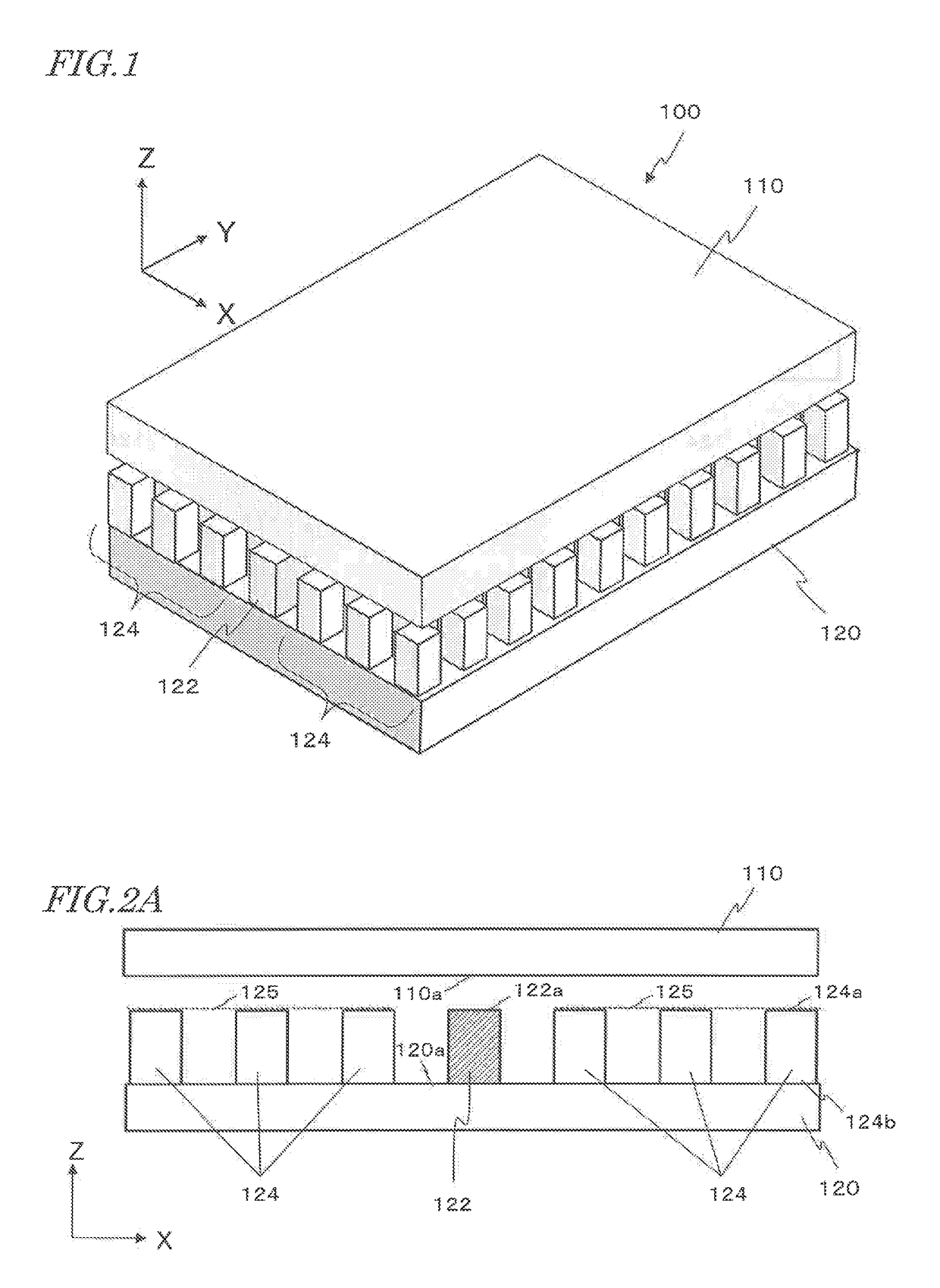
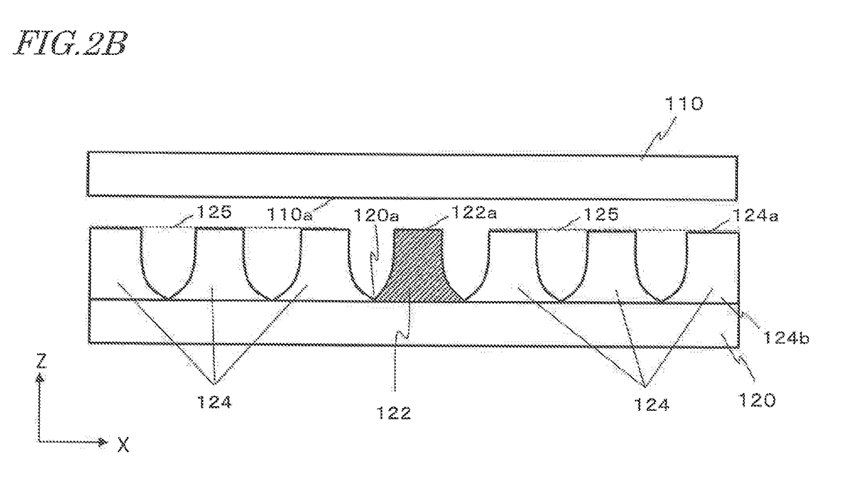
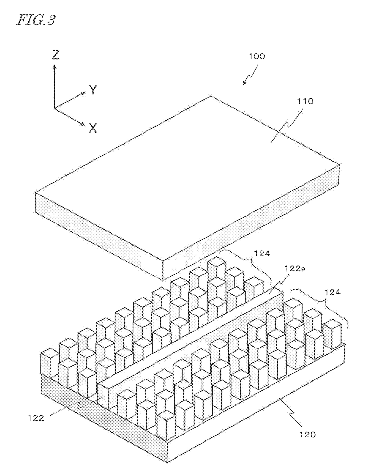
A mounting substrate includes a circuit board and a coupler. The circuit board has a mounting surface on which a microwave integrated circuit element is to be mounted, the microwave integrated circuit element having a plurality of terminals including first and second antenna I/O terminals. The coupler connects the first and second antenna I/O terminals to a waveguide device. The coupler includes: a first electrical conductor portion to be connected to the first antenna I/O terminal; a second electrical conductor portion to be connected to the second antenna I/O terminal; and an elongated gap in which an end face of the first electrical conductor portion and an end face of the second electrical conductor portion oppose each other. The elongated gap has a narrow portion at which the distance between the end face of the first electrical conductor portion and the end face of the second electrical conductor portion is locally decreased. The coupler couples an electromagnetic field being produced at the narrow portion to a waveguide in the waveguide device.

Description

[0001]This is a continuation of International Application No. PCT / JP2017 / 016557, with an international filing date of Apr. 26, 2017, which claims priority of Japanese Patent Application No. 2016-091403, filed on Apr. 28, 2016, the entire contents of which are hereby incorporated by reference.BACKGROUND1. Technical Field[0002]The present disclosure relates to a microwave integrated circuit, a radar device, and a radar system for connection and use with a waveguide device that guides electromagnetic waves by utilizing an artificial magnetic conductor.2. Description of the Related Art[0003]Microwaves (including millimeter waves) for use in a radar system are generated by an integrated circuit which is mounted on a substrate (which herein will be referred to as a “microwave IC”). Depending on the method by which it is produced, a microwave IC may be referred to as an “MIC” (Microwave Integrated Circuit) or an “MMIC” (Monolithic Microwave Integrated Circuit; or Microwave and Millimeter w...

Claims


Application Information

Patent Timeline
IPC IPC(8): H01P5/08H01P3/16H01P5/107H01P5/12
CPCH01P5/087H01P3/16H01P5/107H01P5/12H01Q1/38H01P3/00H01Q1/50H01Q13/00H01Q21/00H05K1/0237
Inventor KIRINO, HIDEKIKAMO, HIROYUKI
Owner NIDEC CORP
Why Eureka
Try Eureka