Exposure device, substrate processing apparatus, exposure method and substrate processing method
a substrate processing and exposure device technology, applied in the direction of instruments, photomechanical devices, optics, etc., can solve the problems of long time and degrade and achieve the effect of degrading the efficiency of the exposure processing of the substra
- Summary
- Abstract
- Description
- Claims
- Application Information
AI Technical Summary
Benefits of technology
Problems solved by technology
Method used
Image
Examples
first embodiment
[1] First Embodiment
[0072](1) Configuration of Exposure Device
[0073]An exposure device, a substrate processing apparatus, an exposure method and a substrate processing method according to embodiments of the present invention will be described below with reference to drawings. In the following description, a substrate refers to a semiconductor substrate, a substrate for an FPD (Flat Panel Display) such as a liquid crystal display device or an organic EL (Electro Luminescence) display device, a substrate for an optical disc, a substrate for a magnetic disc, a substrate for a magneto-optical disc, a substrate for a photomask, a substrate for solar cells or the like.
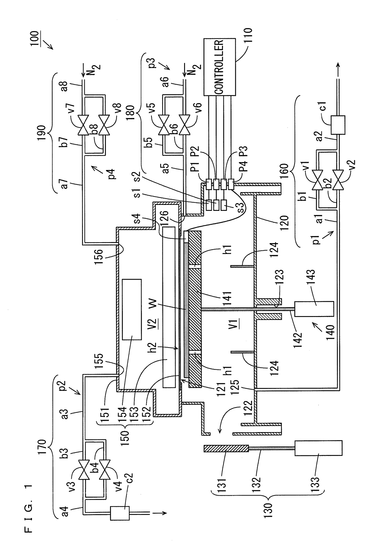
[0074]FIG. 1 is a schematic cross sectional view showing a configuration of the exposure device according to the first embodiment of the present invention. As shown in FIG. 1, the exposure device 100 includes a controller 110, a processing chamber 120, a closing section 130, a lifter-lowerer 140, a light emitter 150, gas exh...
second embodiment
[2] Second Embodiment
[0158]As for an exposure device and a substrate processing apparatus according to the second embodiment, differences from the exposure device and the substrate processing apparatus according to the first embodiment will be described. FIG. 14 is a schematic cross sectional view showing a configuration of the exposure device according to the second embodiment of the present invention. As shown in FIG. 14, the exposure device 100 further includes a connecting pipe 101 that connects a processing chamber 120 to a housing 151. A valve v9 is provided at the connecting pipe 101.
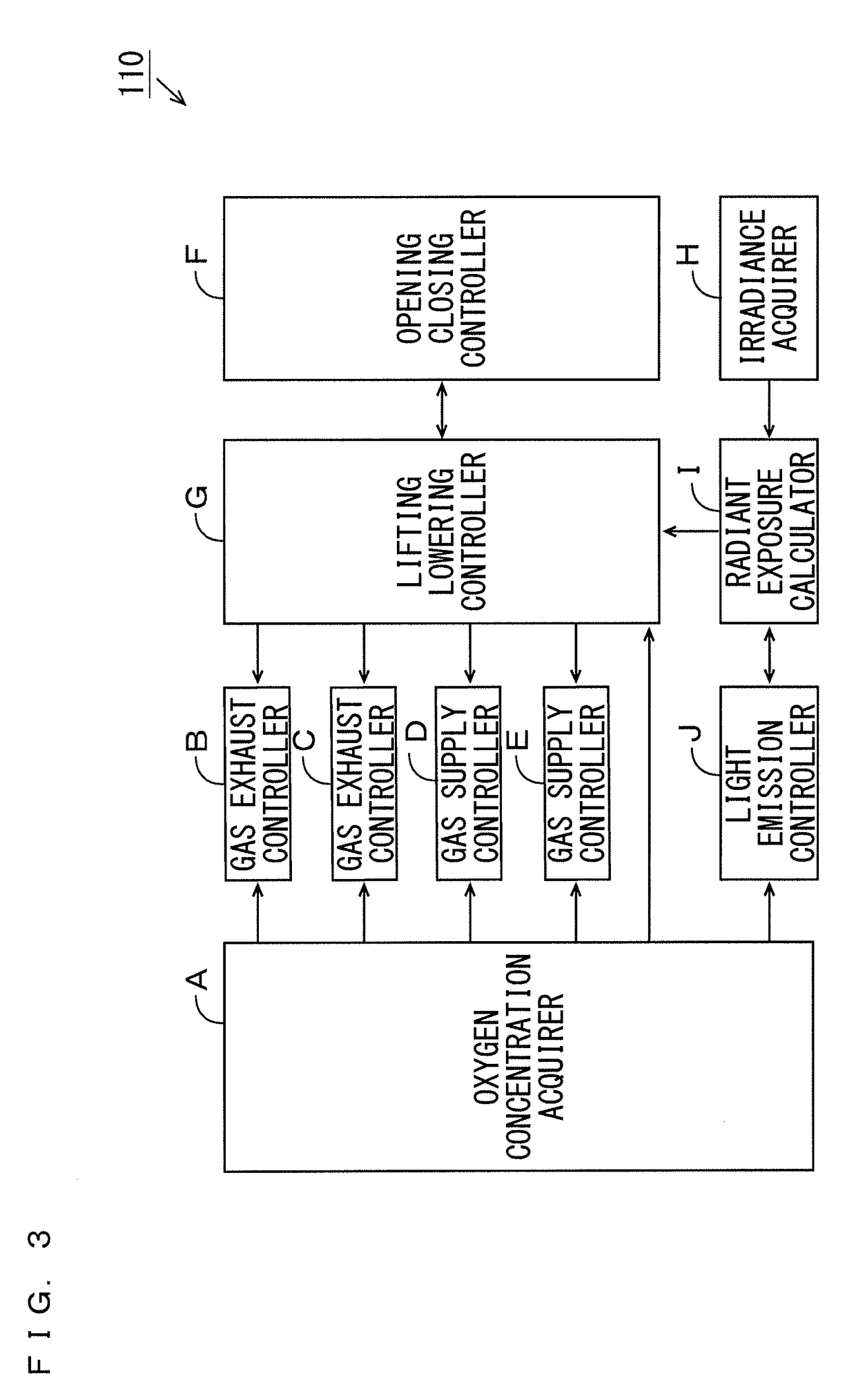
[0159]FIG. 15 is a functional block diagram showing a configuration of a controller 110 of FIG. 14. As shown in FIG. 15, the controller 110 further includes a connection controller K that controls an operation of the valve v9 ofFIG. 14. When the valve v9 is opened, an inner space V1 of the processing chamber 120 and an inner space V2 of the housing 151 communicate with each other through the conn...
PUM
| Property | Measurement | Unit |
|---|---|---|
| wavelength | aaaaa | aaaaa |
| wavelength | aaaaa | aaaaa |
| atmospheric pressure | aaaaa | aaaaa |
Abstract
Description
Claims
Application Information


