Circuit having snubber circuit in power supply device

Inactive Publication Date: 2019-03-28
SPI ELECTRONICS
View PDF82 Cites 14 Cited by
  • Summary
  • Abstract
  • Description
  • Claims
  • Application Information

AI Technical Summary

Benefits of technology

[0004]An objective of the present invention is to provide a transistor structure and a related packaging m

Problems solved by technology

However, the RCD snubber circuit has disadvantages like the high energy loss, poor efficiency and high spike voltage

Method used


Image

  • Circuit having snubber circuit in power supply device
  • Circuit having snubber circuit in power supply device
  • Circuit having snubber circuit in power supply device

Examples


first embodiment

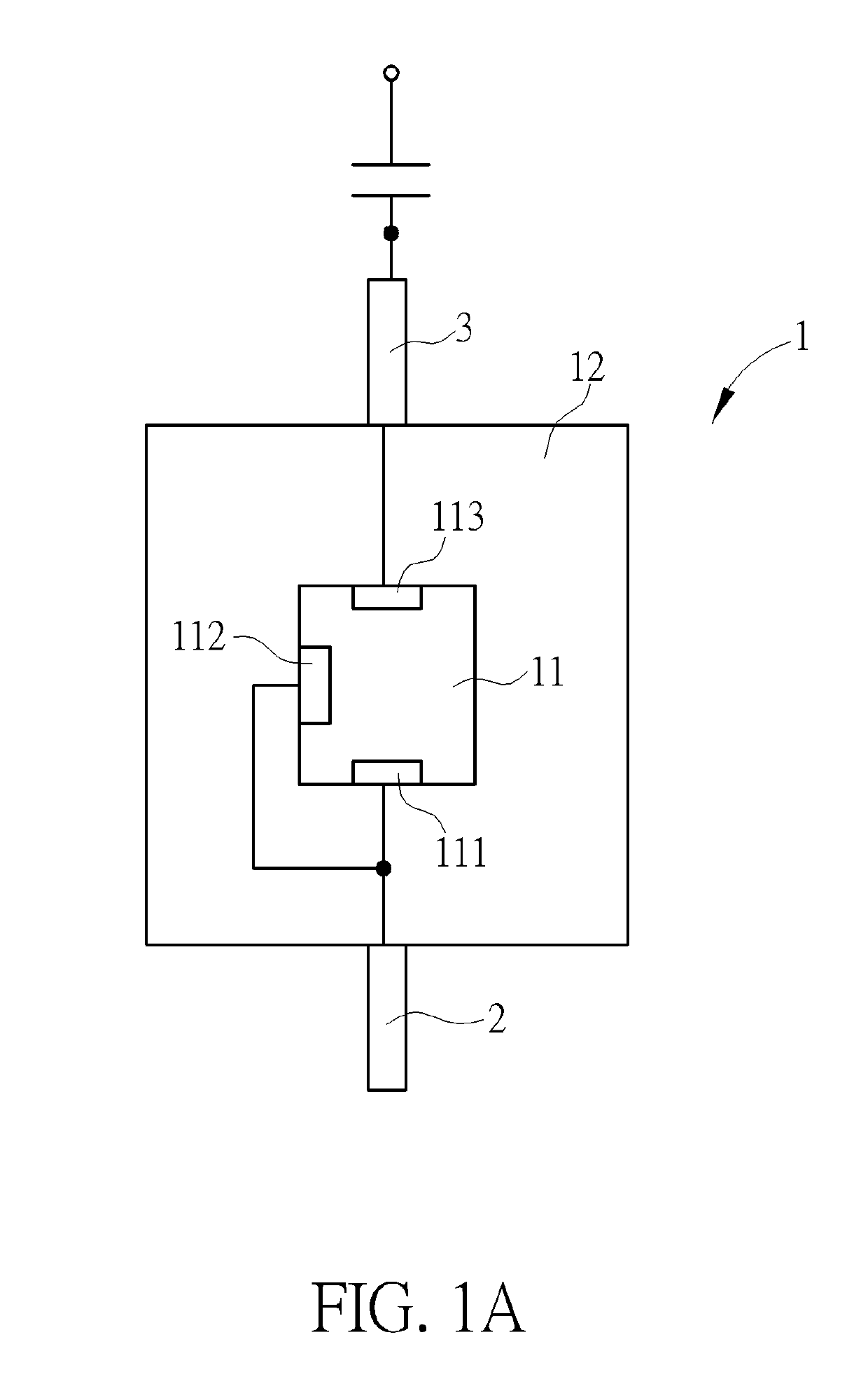
[0061]Please refer to FIG. 1A, which is a diagram illustrating a transistor structure according to the present invention. The transistor structure of the present invention includes a chip package 1 and two pins 2 and 3, wherein the chip package 1 includes a transistor die 11 and a molding compound 12 encapsulating the transistor die 11; and the pin 2 is electrically connected to a first bonding pad 111 and a second bonding pad 112 of the transistor die 11, and the pin 3 is electrically connected to a third bonding pad 113 of the transistor die 11.

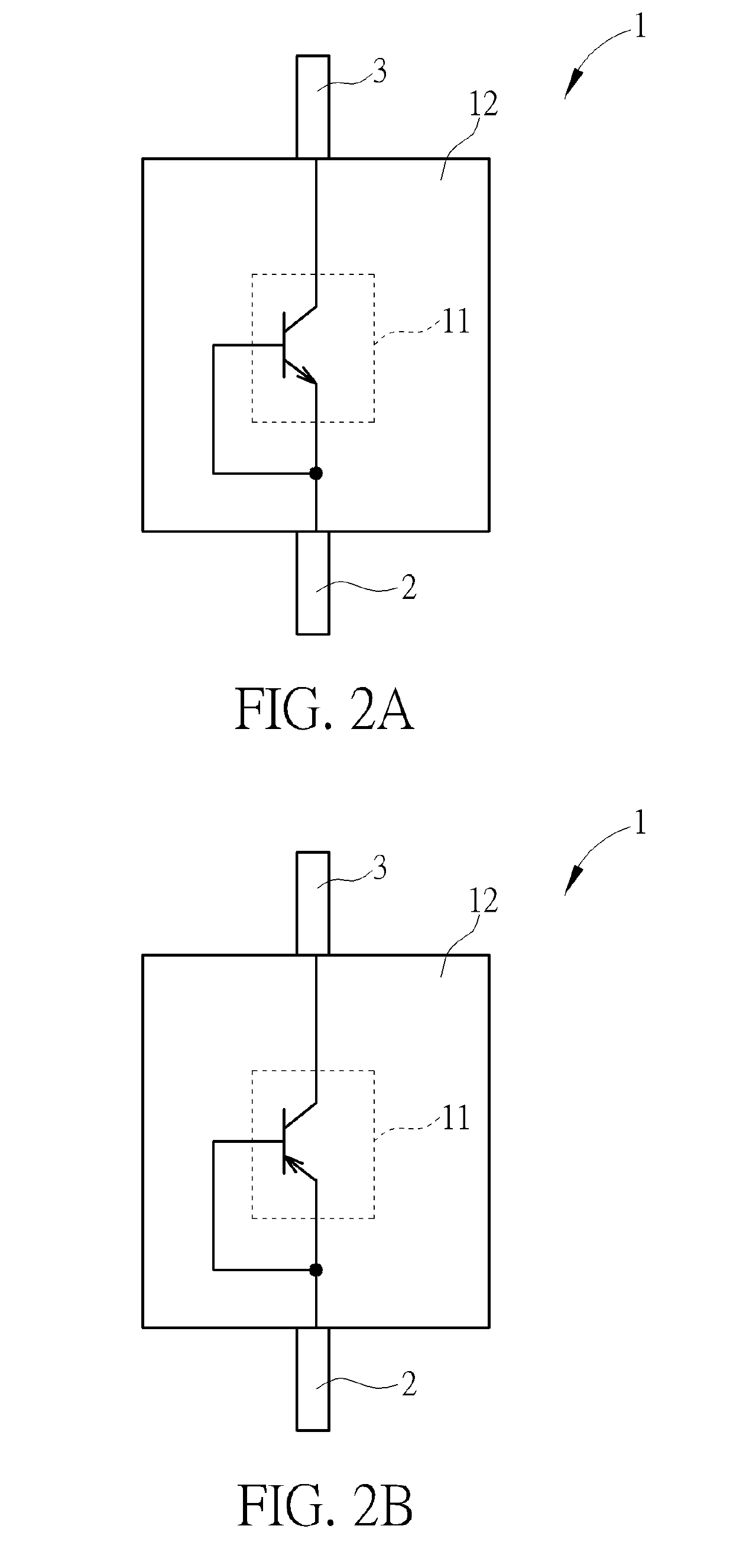
[0062]The transistor die 11 of the transistor structure of the present invention is a Bipolar Junction Transistor (BJT) die, and the BJT may be an NPN type BJT die or a PNP type BJT die. Please refer to FIG. 1A in conjunction with FIG. 2A and FIG. 2B. The first bonding pad 111 of the transistor die 11 is an emitter bonding pad, and the second bonding pad 112 is a base bonding pad, and the third bonding pad 113 is a collector bonding pad, wh...

second embodiment

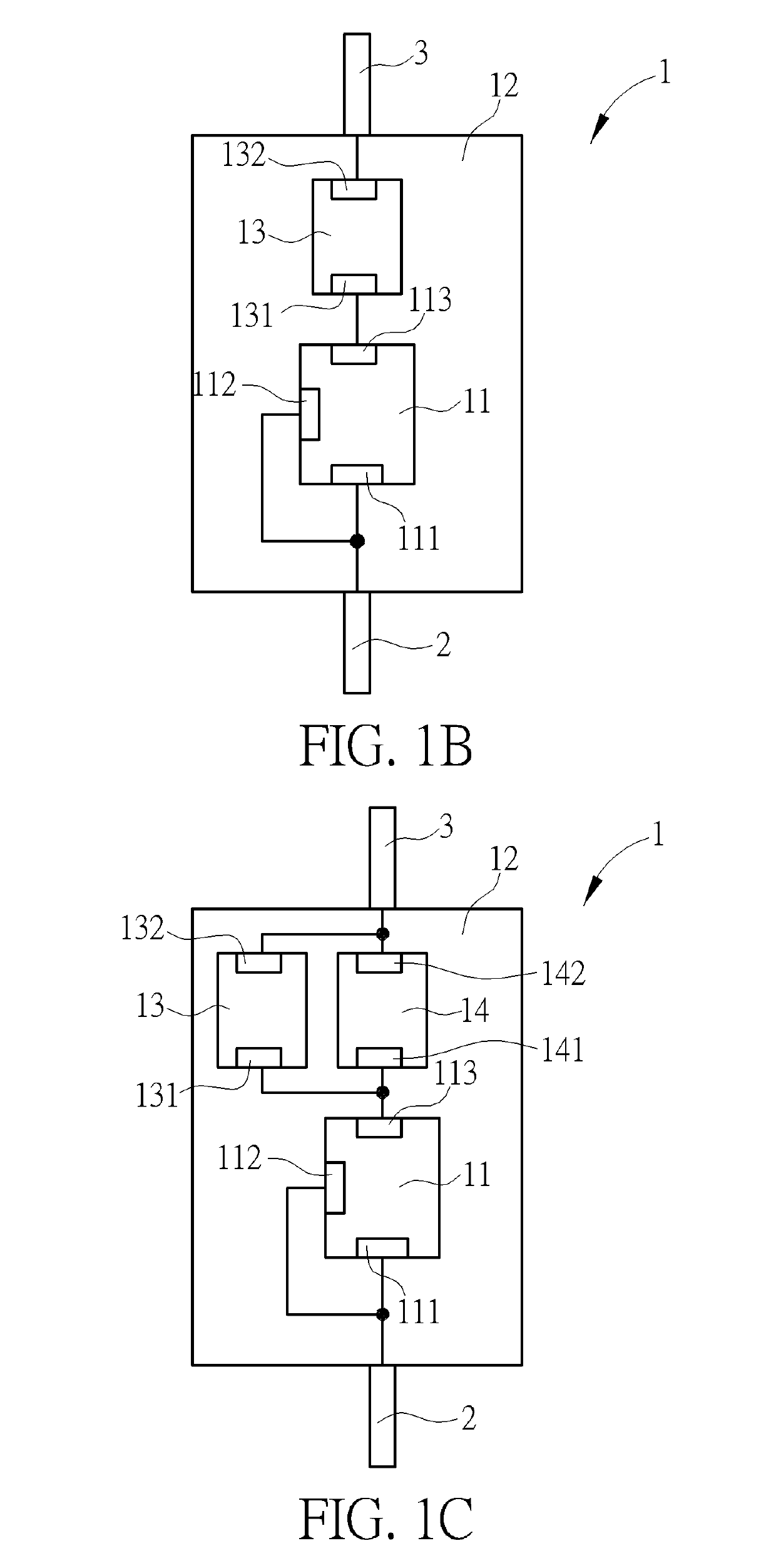
[0072]Please refer to FIG. 1B, which is a diagram illustrating a transistor structure according to the present invention. The transistor structure of the present invention includes a chip package 1 and two pins 2 and 3, wherein the chip package 1 includes a transistor die 11, a capacitor die 13, and a molding compound12 encapsulating the transistor die 11 and the capacitor die 13. The third bonding pad 113 of the transistor die 11 is electrically connected to a first bonding pad 131 of the capacitor die 13. The pin 2 is electrically connected to a first bonding pad 111 and the second bonding pad 112 of the transistor die 11, and the pin 3 is electrically connected to a second bonding pad 132 of the capacitor die 13. The transistor structure of this embodiment may make the first bonding pad 111 (or the second bond 112) of the transistor die 11 electrically connected to the first bonding pad 131 of the capacitor die 13, may make the pin 2 electrically connected to the second bonding p...

third embodiment

[0075]Please refer to FIG. 10, which is a diagram illustrating the transistor structure according to the present invention. The transistor structure of the present invention includes a chip package 1 and two pins 2 and 3, wherein the chip package 1 includes a transistor die 11, a capacitor die 13, a zener diode die 14, and a molding compound 12 encapsulating the transistor die 11, the capacitor die 13, and the zener diode die 14. The third bonding pad 113 of the transistor die 11 is electrically connected to a first bonding pad 131 of the capacitor die 13 and a first bonding pad 141 of the zener diode die 14. The pin 2 is electrically connected to a first bonding pad 111 and the second bonding pad 112 of the transistor die 11, and the pin 3 is electrically connected to a second bonding pad 132 of the capacitor die 13 and a second bonding pad 142 of the zener diode die 14. The transistor structure of this embodiment may make the first bonding pad 111 and the second bonding pad 112 of...


PUM


Abstract

A snubber circuit is provided. The snubber circuit includes a transistor structure and a first capacitor. The transistor structure includes a chip package and two pins. The chip package includes a transistor die and a molding compound encapsulating the transistor die. A first pin of the two pins is electrically connected to a first bonding pad and a second bonding pad of the transistor die, and a second pin of the two pins is electrically connected to a third bonding pad of the transistor die. The first pin or the second pin of the transistor structure is electrically connected to a terminal of the first capacitor.

Description

CROSS REFERENCE TO RELATED APPLICATIONS[0001]This is a continuation-in-part of U.S. application Ser. No. 15 / 166,236 (filed on May 26, 2016), which is a continuation-in-part of U.S. application Ser. No. 13 / 612,867 (filed on Sep. 13, 2012). U.S. application Ser. No. 13 / 612,867 claims the benefit of U.S. provisional application No. 61 / 533,796 (filed on Sep. 13, 2011) and U.S. provisional application No. 61 / 682,319 (filed on Aug. 13, 2012). The entire contents of the related applications, including U.S. application Ser. No. 15 / 166,236, U.S. application Ser. No. 13 / 612,867, U.S. provisional application No. 61 / 533,796 and U.S. provisional application No. 61 / 682,319, are included herein by reference.BACKGROUND OF THE INVENTION1. Field of the Invention[0002]The present invention relates to a snubber circuit, and more particularly, to a snubber circuit including a transistor structure with two pins and related packaging method thereof.2. Description of the Prior Art[0003]In recent years, due...

Claims


Application Information

Patent Timeline
IPC IPC(8): H02M1/34H01L25/16H01L23/00
CPCH02M1/34H01L25/16H01L24/09H01L24/49H01L24/73H01L2924/1305H01L2924/12035H01L2924/1205H01L2924/181H01L23/49562H01L24/45H01L2224/16245H01L2224/32245H01L2224/45144H01L2224/48091H01L2224/48247H01L2224/73265H01L2924/13091H01L2924/13055H01L23/66H01L23/642H01L24/29H01L24/13H01L24/16H01L24/32H01L24/48H01L2224/1703H01L2224/16106H01L2224/13111H01L2224/29199H01L2224/29339Y02B70/10H02M1/342H01L2924/00014H01L2924/00012H01L2924/00
Inventor LIN, KUO-FAN
Owner SPI ELECTRONICS
Why Eureka
Try Eureka