Resistive random access memory device for 3D stack and memory array using the same and fabrication method thereof

Active Publication Date: 2019-05-02
SEOUL NAT UNIV R&DB FOUND
View PDF0 Cites 5 Cited by
  • Summary
  • Abstract
  • Description
  • Claims
  • Application Information

AI Technical Summary

Benefits of technology

[0021]The present invention, by forming a bottom electrode from a doped semiconductor, can be fabricated simultaneously with peripheral circuit elements due to the compatibility with the conventional CMOS process. By having one or more electric field concentration regions in the bottom electrode,

Problems solved by technology

However, in recent years, as the size of the device has been reduced to 20 nm or less, several reliability problems have arisen.
In particular, a unipolar RRAM operating as shown in FIG. 3A has a disadvantage for commercialization in that the dispersion of the switching parameters is uneven and the reset current is high.
The leakage current of these adjacent cells 430 and 440 has been the caus

Method used


Image

  • Resistive random access memory device for 3D stack and memory array using the same and fabrication method thereof
  • Resistive random access memory device for 3D stack and memory array using the same and fabrication method thereof
  • Resistive random access memory device for 3D stack and memory array using the same and fabrication method thereof

Examples


Embodiment Construction

[0033]Detailed descriptions of preferred embodiments of the present invention are provided below with accompanying drawings.

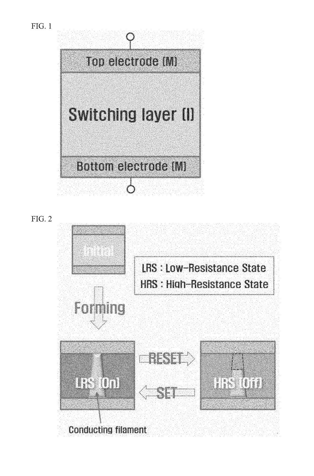
[0034]First, referring to FIG. 10 and FIG. 17, a resistive memory device of the present invention will be described.

[0035]A resistive memory device according to the present invention comprises, as commonly shown in FIGS. 10 and 17, a bottom electrode 21 or 24 formed by doping impurities into a semiconductor material; a resistance change layer 30 or 50 formed on the bottom electrode; and a top electrode 40 formed on the resistance change layer, wherein the bottom electrode 21 or 24 has one or more electric field concentration regions A, B, C and D, or E toward the resistance change layer 30 or 50.

[0036]Here, the semiconductor material forming the bottom electrode 21 or 24 may be any material as long as it can be made conductive by doping with impurities. However, materials such as a semiconductor material used in making circuit elements as well as the memory dev...


PUM


Abstract

The present invention relates to a resistance change memory, that is, a resistive memory device. By forming a bottom electrode from a doped semiconductor different material from a conventional one, it is possible to fabricate the memory device simultaneously with peripheral circuit elements. By having one or more electric field concentration regions in the bottom electrode, it is possible to reduce the power consumption reducing the voltage. The present invention can be also stacked vertically in any small and apply to the synaptic device array recently attracting the great interest as the next generation computing technology for realizing the neural imitation system.

Description

CROSS-REFERENCE TO RELATED APPLICATION[0001]This application claims priority to Korean Patent Application No. 10-2017-0142238, filed on Oct. 30, 2017, under 35 U.S.C. 119, the entire contents of which are hereby incorporated by reference.BACKGROUNDField of the Invention[0002]The present invention relates to a resistive switching memory, or resistive random access memory (RRAM) device, and more particularly to a resistive memory device for three-dimensional stacking, a memory array using the same and a fabrication method thereof.Related Art[0003]NAND flash memory technology is currently leading the mass storage market through continuously scaling down. However, in recent years, as the size of the device has been reduced to 20 nm or less, several reliability problems have arisen. Therefore, various kinds of next generation memories are being actively researched to replace NAND flash memory technology.[0004]The RRAM having the simplest structure among them is advantageous for miniaturi...

Claims


Application Information

Patent Timeline
IPC IPC(8): H01L45/00
CPCH01L45/1273H01L45/16H01L45/08H01L45/145H01L45/1226H10B63/845H10N70/821H10N70/823H10N70/20H10N70/8418H10N70/883H10N70/011H10N70/8833H10N70/841H10N70/826H10N70/24
Inventor PARK, BYUNG-GOOKKIM, SUNGJUNKIM, MIN-HWIKIM, TAE-HYEONLEE, SANG-HO
Owner SEOUL NAT UNIV R&DB FOUND
Why Eureka
Try Eureka