Method of selectively depositing a capping layer structure on a semiconductor device structure

a semiconductor device and capping layer technology, applied in semiconductor devices, semiconductor/solid-state device details, electrical equipment, etc., can solve the problems of copper having certain characteristics, low electrical resistivity and durability, and copper diffraction into adjacent materials

Active Publication Date: 2019-05-16
ASM IP HLDG BV
View PDF8 Cites 248 Cited by
  • Summary
  • Abstract
  • Description
  • Claims
  • Application Information

AI Technical Summary

Problems solved by technology

One metallic interconnect material that is currently utilized is copper, due to copper's low electrical resistivity and durability.
However, copper has certain disadvantages, particularly the capability of copper to diffuse

Method used


Image

  • Method of selectively depositing a capping layer structure on a semiconductor device structure
  • Method of selectively depositing a capping layer structure on a semiconductor device structure
  • Method of selectively depositing a capping layer structure on a semiconductor device structure

Examples


Embodiment Construction

[0018]Although certain embodiments and examples are disclosed below, it will be understood by those in the art that the invention extends beyond the specifically disclosed embodiments and / or uses of the invention and obvious modifications and equivalents thereof. Thus, it is intended that the scope of the invention disclosed should not be limited by the particular disclosed embodiments described below.

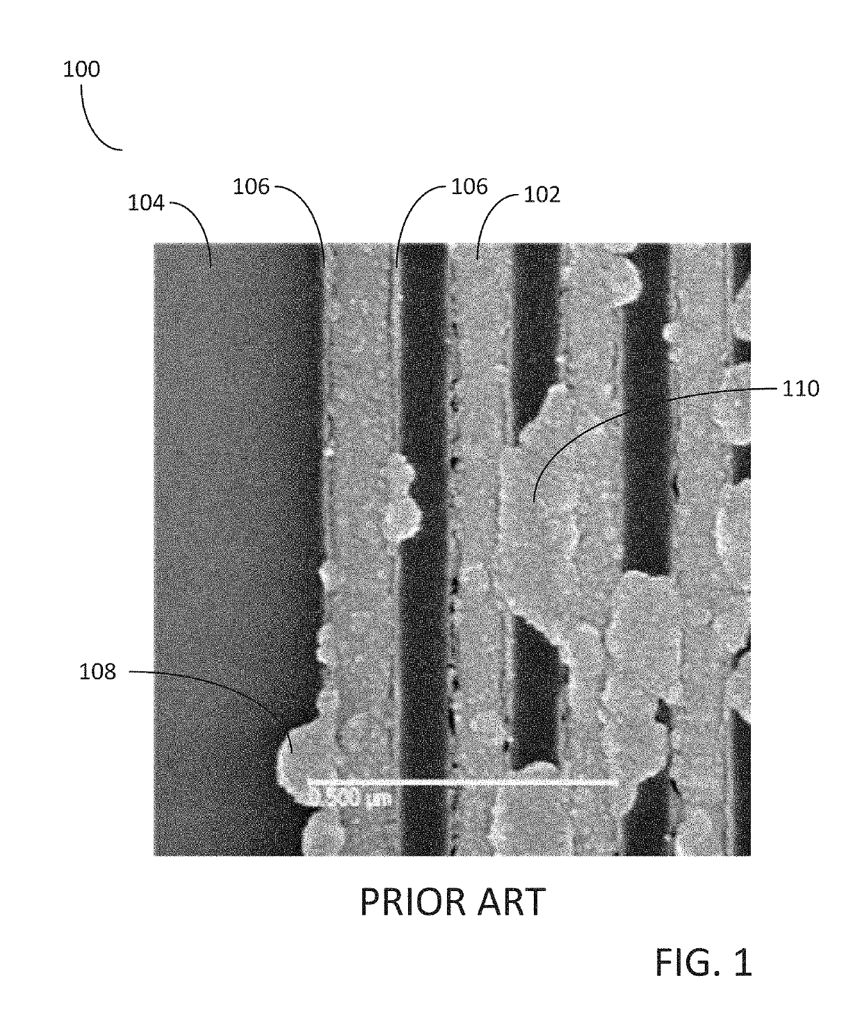
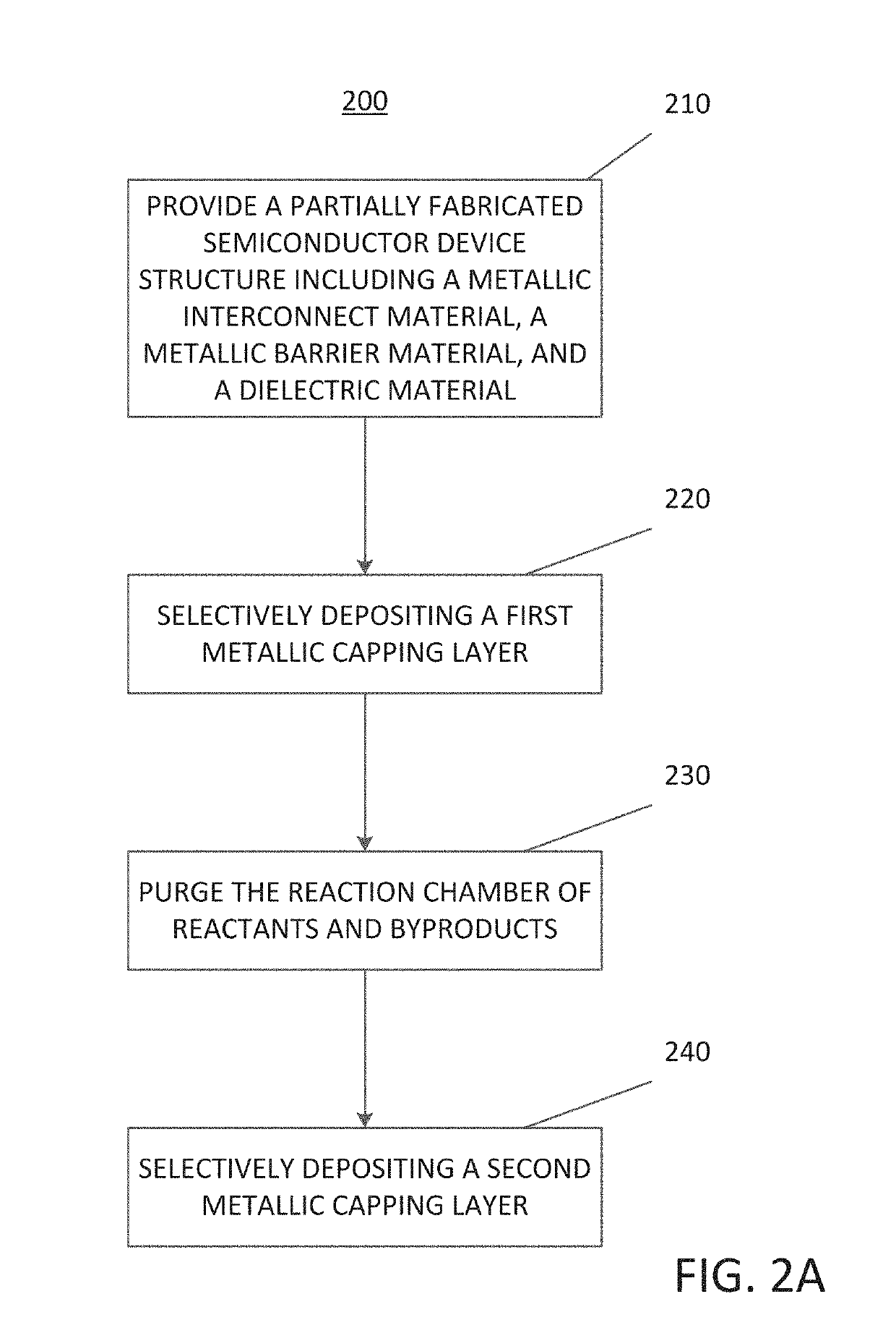
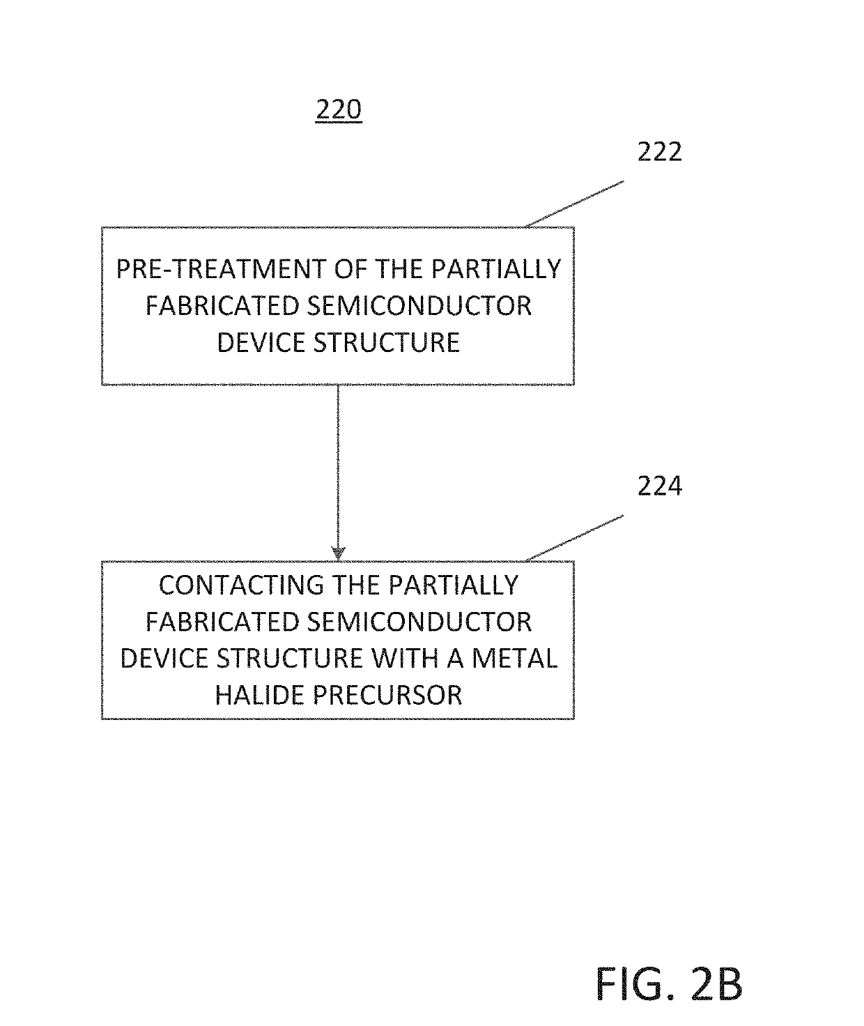
[0019]The illustrations presented herein are not meant to be actual views of any particular material, structure, or device, but are merely idealized representations that are used to describe embodiments of the disclosure.

[0020]As used herein, the term “semiconductor device structure” may refer to any portion of a processed semiconductor structure that is, includes, or defines at least a portion of an active or passive component of a semiconductor device to be formed on or in a semiconductor substrate. For example, semiconductor device structures may include, active and passive componen...


PUM


Abstract

A method of selectively depositing a capping layer structure on a semiconductor device structure is disclosure. The method may include; providing a partially fabricated semiconductor device structure comprising a surface including a metallic interconnect material, a metallic barrier material, and a dielectric material. The method may also include; selectively depositing a first metallic capping layer over the metallic barrier material and over the metallic interconnect material relative to the dielectric material; and selectively depositing a second metallic capping layer over the first metallic capping layer relative to the dielectric material. Semiconductor device structures including a capping layer structure are also disclosed.

Description

FIELD OF INVENTION[0001]The present disclosure relates generally to methods for selectively depositing a capping layer structure on a semiconductor device structure and particularly methods for selectively depositing a metallic capping layer structure over a partially fabricated semiconductor device structure comprising a surface including a metallic interconnect material, a metallic barrier material, and a dielectric material.BACKGROUND OF THE DISCLOSURE[0002]Aluminum as a metallic interconnect material in integrated semiconductor circuits has essentially been replaced with alternative metallic interconnect materials primarily due to aluminums high electrical resistivity. One metallic interconnect material that is currently utilized is copper, due to copper's low electrical resistivity and durability. However, copper has certain disadvantages, particularly the capability of copper to diffuse into adjacent materials, such as adjacent, surrounding dielectric materials. Due to the dif...

Claims


Application Information

Patent Timeline
IPC IPC(8): H01L21/768H01L21/285H01L23/532
CPCH01L21/76849H01L21/76847H01L21/76846H01L21/28562H01L23/53238H01L21/7685
Inventor KURODA, AURELIEKOBAYASHI, AKIKOISHIKAWA, DAI
Owner ASM IP HLDG BV
Why Eureka
Try Eureka