Active load generation circuit and filter using same

a technology of active load generation and filter, which is applied in the field of active load generation circuit and filter, can solve the problems of reducing the area of passive components, increasing the risk of producing impedances which are relatively unsusceptible to process, voltage and temperature, etc., and achieves a small area and high impedance.

Active Publication Date: 2019-05-16
REALTEK SEMICON CORP
View PDF4 Cites 3 Cited by
  • Summary
  • Abstract
  • Description
  • Claims
  • Application Information

AI Technical Summary

Benefits of technology

[0008]The active load generation circuit of the present invention can provide a high impedance with a small area and is suitable for being implemented in ICs. Compared with the prior art, the impedance of the active load generation circuit of the present invention is less susceptible to the process, voltage, and temperature. In addition, the filter using the active load generation circuit of the present invention not only saves the pins, but also occupies a smaller circuit area for the same cutoff frequency.

Problems solved by technology

Passive components (e.g., resistors and capacitors) are commonly used in modern integrated circuits (ICs) but often occupy a large area.
In the applications of modern ICs, the circuit area is becoming more and more critical; thus reducing the area of passive components becomes an important issue.
For the circuit design of FIG. 1B, although no extra pin of the chip is taken, the resistor R must be made relatively large to achieve the same cutoff frequency fc because it is undesirable to manufacture a large on-chip capacitor.
Although active components can be used to replace passive components such as resistors to save area, the impedances of active components are more susceptible to process, voltage, and temperature, compared to passive resistors.
Therefore, to produce impedance which is relatively unsusceptible to process, voltage, and temperature in a chip (i.e., IC) becomes an important issue.

Method used


Image

  • Active load generation circuit and filter using same
  • Active load generation circuit and filter using same
  • Active load generation circuit and filter using same

Examples


Embodiment Construction

[0022]The following description is written by referring to terms of this technical field. If any term is defined in this specification, such term should be explained accordingly. In addition, the connection between objects or events in the below-described embodiments can be direct or indirect provided that these embodiments are practicable under such connection. Said “indirect” means that an intermediate object or a physical space exists between the objects, or an intermediate event or a time interval exists between the events.

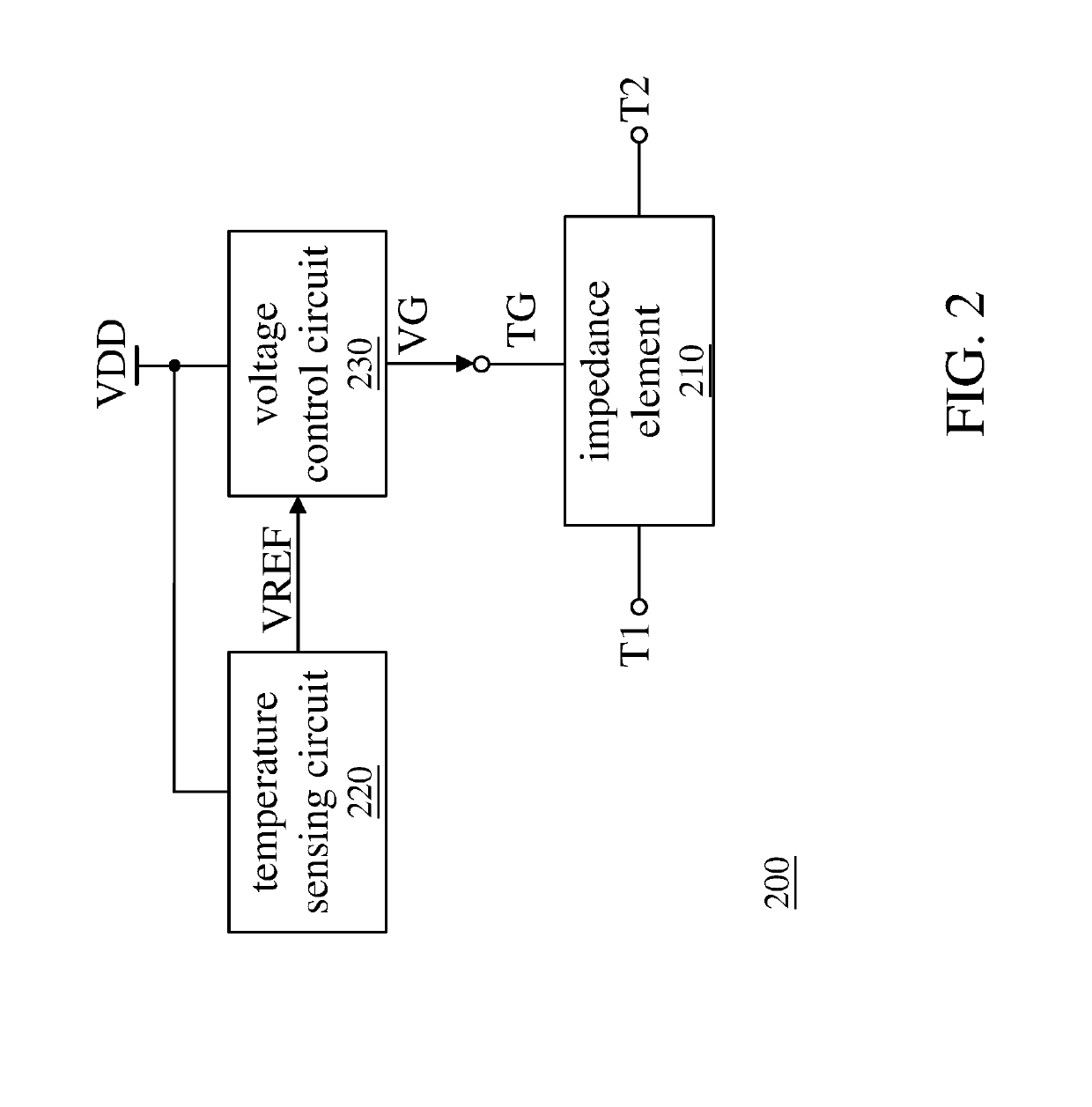
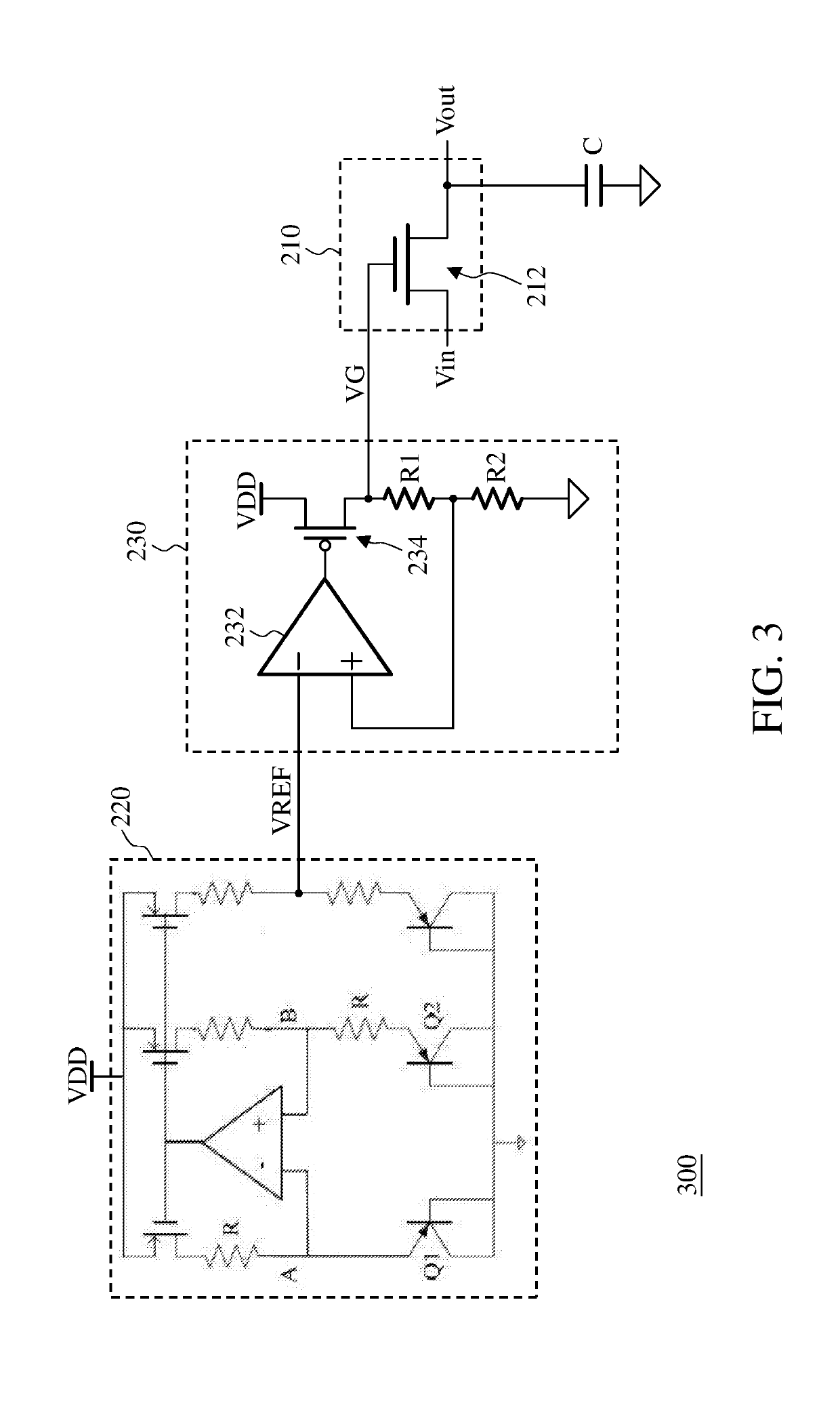
[0023]The disclosure herein includes an active load generation circuit and a filter using same. On account of that some or all elements of the active load generation circuit and the filter could be known, the detail of such elements is omitted provided that such detail has little to do with the features of this disclosure and this omission nowhere dissatisfies the specification and enablement requirements. A person having ordinary skill in the art can choose c...


PUM


Abstract

This invention discloses an active load generation circuit and a filter. The active load generation circuit includes a transistor, a voltage control circuit, a voltage offset and tracking circuit, and a temperature sensing circuit. The transistor provides an impedance and includes a control terminal and an input terminal. The control terminal receives a control voltage, the input terminal receives an input signal, and the impedance is associated with the control voltage. The voltage control circuit generates an intermediate voltage according to a power supply voltage and a first reference voltage. The voltage offset and tracking circuit generates the control voltage according to the input signal and the intermediate voltage such that the control voltage varies with the input signal. The temperature sensing circuit senses an ambient temperature of the active load generation circuit and adjusts the first reference voltage according to the ambient temperature.

Description

BACKGROUND OF THE INVENTION1. Field of the Invention[0001]The present invention relates to on-chip impedance, and, more particularly, to an active load generation circuit and a filter employing the same.2. Description of Related Art[0002]Passive components (e.g., resistors and capacitors) are commonly used in modern integrated circuits (ICs) but often occupy a large area. In the applications of modern ICs, the circuit area is becoming more and more critical; thus reducing the area of passive components becomes an important issue. Taking the filter commonly seen in the circuits as an example, in the circuit of FIG. 1A, the resistor R is fabricated inside the chip (on-chip), whereas the capacitor C is disposed outside the chip (off-chip) and connected with the resistor R through the pin 110 of the chip. In the circuit of FIG. 1B, both the resistor R and the capacitor C are fabricated inside the chip. The input signal Sin, which is a voltage signal or a current signal, is filtered by t...

Claims


Application Information

Patent Timeline
Patent Type & Authority Applications(United States)
IPC IPC(8): H03K17/14H03K17/22H03L1/04H01L23/64
CPCH03K17/145H03K17/223H03L1/04H01L23/64H03K2017/0806H03K19/0005H03H11/53H03H11/54
Inventor TANG, WEI-CHENGWU, KUOHSI
Owner REALTEK SEMICON CORP
Why Eureka
Try Eureka