Optical Assembly and Display Device

Active Publication Date: 2019-05-23
OSRAM OLED
View PDF6 Cites 3 Cited by
  • Summary
  • Abstract
  • Description
  • Claims
  • Application Information

AI Technical Summary

Benefits of technology

The patent is about using chip groups with many light emitting diode chips to replace individual RGB LED chips in display devices. This improves resolution and makes it more difficult to see the placement of the chips.

Problems solved by technology

Previous optical assemblies for display devices, for example, used prisms or microlens arrays, which can lead to undesirable distortions in the image display.
The beam guidance is often complex and limited by the dense grouping of the light emitting diode chips on a common carrier.

Method used


Image

  • Optical Assembly and Display Device
  • Optical Assembly and Display Device
  • Optical Assembly and Display Device

Examples


Embodiment Construction

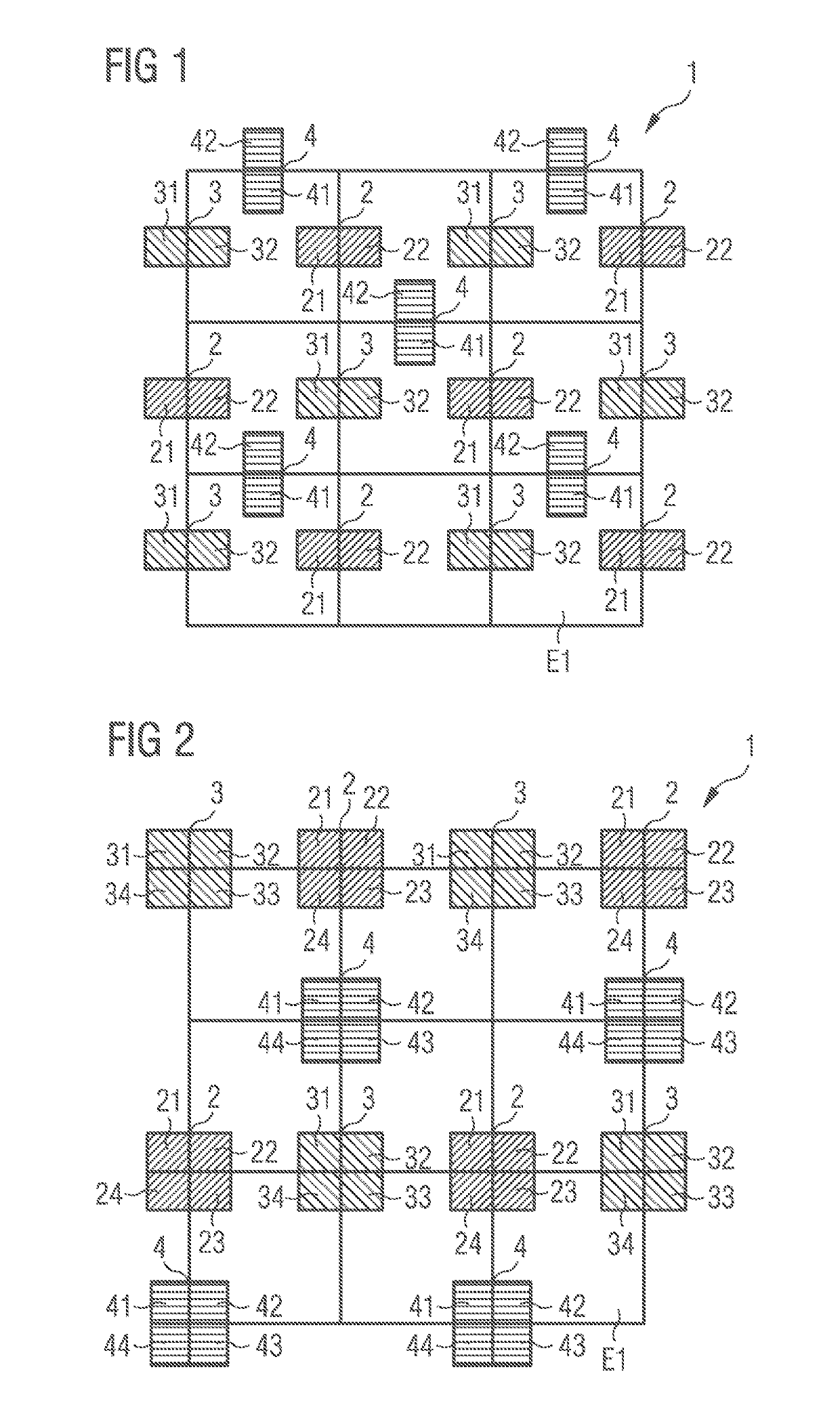
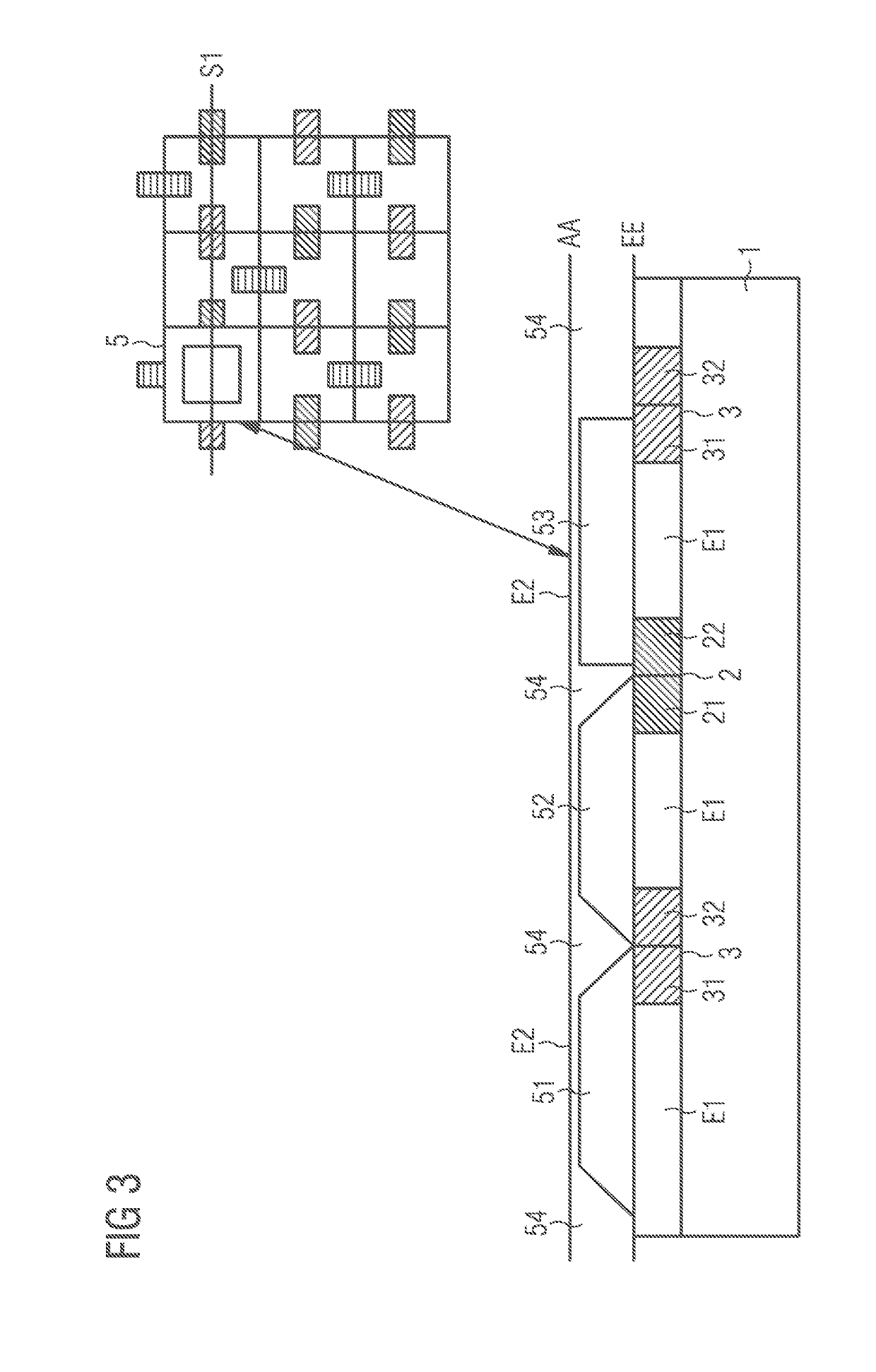
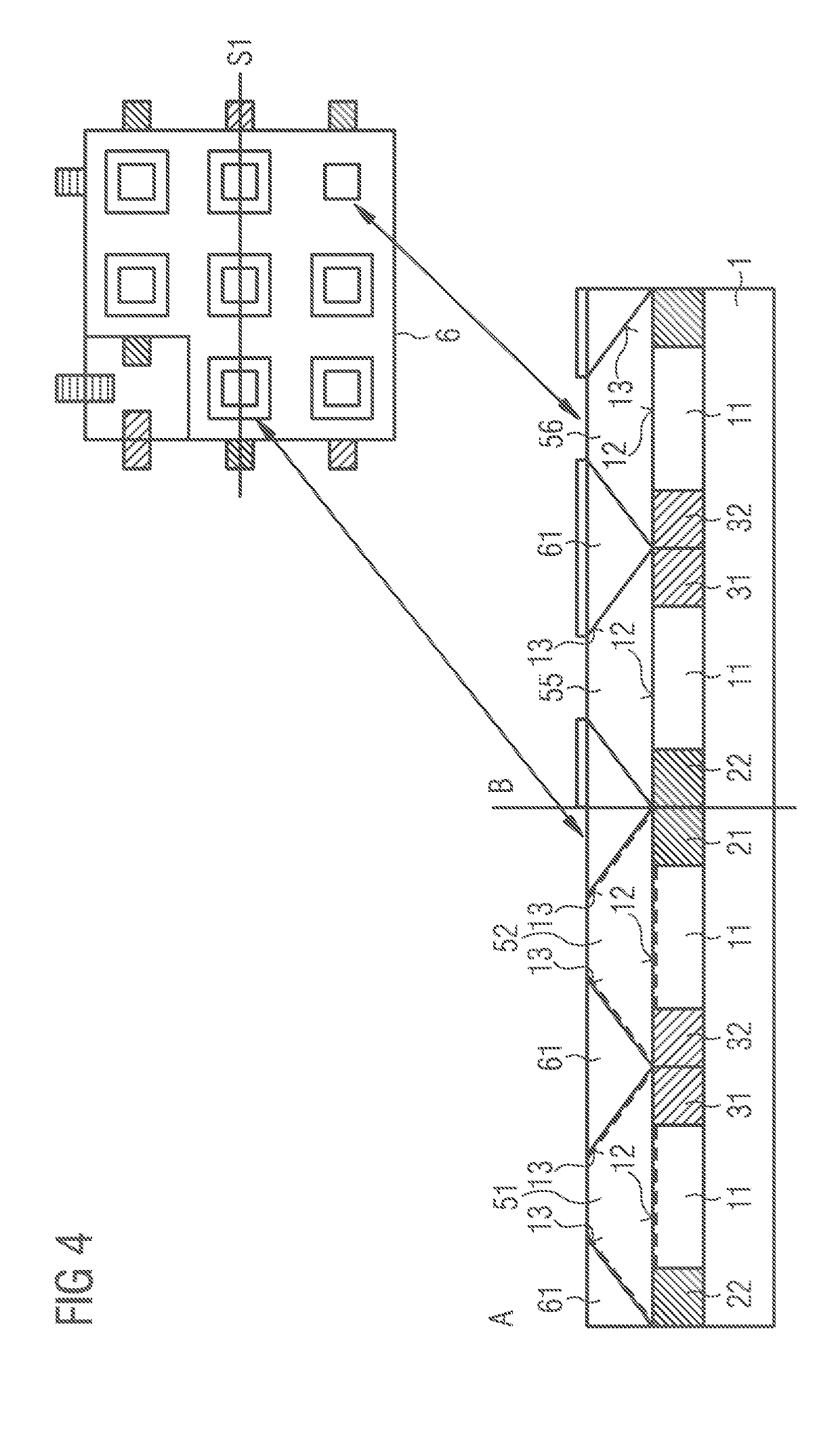
[0052]FIG. 1 shows an exemplary embodiment of an optical assembly. On a common carrier 1 several luminescence diode chips 21, 22, 31, 32, 41, 42 are each arranged planar in chip groups 2, 3, 4. Each of the chip groups comprises two similar luminescence diode chips 21 and 22, 31 and 32, or 41 and 42. Similar luminescence diode chips are each designed to emit substantially the same colors. For example, first chip groups 2 each comprise red emitting luminescence diode chips 21, 22. Second chip groups 3 each include green emitting luminescence diode chips 31, 32, and third chip groups 4 each include blue emitting luminescence diode chips 41, 42.

[0053]The chip groups, and thus the luminescence diode chips, are arranged along a grid in unit cells E1 on the carrier 1. Parallel to the grid there is an input plane EE in which the first unit cells come to rest. In each unit cell E1 there are different luminescence diode chips each from three different chip groups. For example, a single unit c...


PUM


Abstract

An optical assembly and a display device are disclosed. In an embodiment an optical assembly includes a common carrier, a plurality of first chip groups, each first chip group comprising at least two similar luminescence diode chips, a plurality of second chip groups, each second chip group comprising at least two similar luminescence diode chips, wherein the first and second chip groups are arranged planar along a regular grid of first unit cells on a main surface of the common carrier and an optical element arranged downstream of the first and second chip groups with respect to a main radiation direction, wherein the luminescence diode chips of the different chip groups are configured to emit electromagnetic radiation of different wavelength characteristics.

Description

[0001]This patent application is a national phase filing under section 371 of PCT / EP2017 / 061345, filed May 11, 2017, which claims the priority of German patent application 10 2016 108 776.9, filed May 12, 2016, each of which is incorporated herein by reference in its entirety.TECHNICAL FIELD[0002]This invention relates to an optical assembly.SUMMARY OF THE INVENTION[0003]Modern display devices such as displays are often based on an arrangement of a large number of light emitting diode chips, which are combined in a multichip component for use as a display, such as a narrow pixel pitch video wall module. Here, for example, the idea is being pursued of replacing individual red, green, blue (RGB) LED chips with chip groups each with a large number of light emitting diode chips of the same color. This will make it possible to avoid the restrictions caused by the chips being placed on the chip carrier and achieve a higher density and thus a higher resolution.[0004]Previous optical assemb...

Claims


Application Information

Patent Timeline
IPC IPC(8): H01L27/15H01L25/075H01L33/58H01L33/62
CPCH01L27/156H01L25/0753H01L33/58H01L33/62H01L33/08
Inventor BRICK, PETERSABATHIL, MATTHIASSINGER, FRANKSCHWARZ, THOMAS
Owner OSRAM OLED
Why Eureka
Try Eureka