TFT structure based on flexible multi-layer graphene quantum carbon substrate material and method for manufacturing same

Active Publication Date: 2019-05-23
GUANG DONG DONGBOND TECH CO LTD
View PDF4 Cites 1 Cited by
  • Summary
  • Abstract
  • Description
  • Claims
  • Application Information

AI Technical Summary

Benefits of technology

The present invention provides a method for preparing a flexible graphene material with small in-plane dispersion and deviation degree. The material has a great curvature and can be used for the preparation of high-performance field effect transistors and quantum computing chip semiconductors. The method involves carbonizing and graphitizing a PI film to form a microcrystalline carbon precursor, which is then doped with nano-metallic material to form quantum dots. The resulting material has a unique structure with hexagonal planar network molecular structures arranged in order. The method also allows for large-area, roll-to-roll, continuous batch production at low costs.

Problems solved by technology

Electrical characteristics of a device suffer serious deterioration under an applied voltage and an illumination condition, with a result that the amorphous silicon TFT technology cannot adapt to requirements of a novel flexible display technology.
However, a process for preparing low temperature poly-silicon is relatively complicated, the process temperature is high, and large-area uniformity has a problem.
However, at present, there is still a long way to apply organic TFTs commercially on a large scale mainly because a device is highly sensitive to vapor in atmosphere and temperature and stability of the device needs to be further improved.

Method used


Image

  • TFT structure based on flexible multi-layer graphene quantum carbon substrate material and method for manufacturing same
  • TFT structure based on flexible multi-layer graphene quantum carbon substrate material and method for manufacturing same

Examples


Embodiment Construction

[0061]Preferred embodiments of the present invention are further described in detail below.

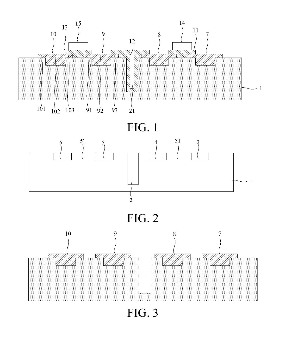
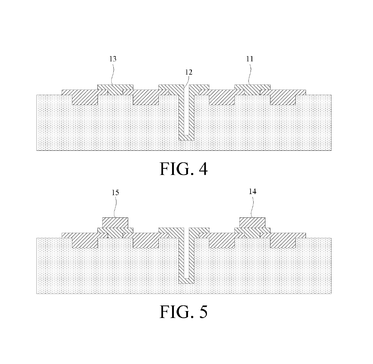
[0062]As shown in FIG. 1 to FIG. 5, a thin film transistor (TFT) structure based on a flexible multi-layer graphene quantum carbon substrate material according to an embodiment includes a multi-layer graphene quantum carbon substrate 1, a first source 10, a first drain 9, a first gate insulating layer 13, and a first gate 15, a second source 8, a second drain 7, a second gate insulating layer 11, and a second gate 14. The multi-layer graphene quantum carbon substrate includes a first channel area 51, a second channel area 31, and a first drain area 5, a first source area 6, a second drain area 3, a second source area 4, and an isolation area 2 that are located at corresponding recessed positions on the multi-layer graphene quantum carbon substrate 1 that are separated from each other. The first channel area 51 is located between the first drain area 5 and the first source area 6. The first sou...


PUM


Abstract

A TFT structure based on a flexible multi-layer graphene quantum carbon substrate material and a method for manufacturing the same. The TFT structure includes a multi-layer graphene quantum carbon substrate, a first source, a first drain, a first gate insulating layer, and a first gate. The multi-layer graphene quantum carbon substrate includes a first channel area, and a first drain area and a first source area that are located at corresponding recessed positions on the multi-layer graphene quantum carbon substrate that are separated from each other. The first channel area is located between the first drain area and the first source area, the first source is filled in the first source area, the first drain is filled in the first drain area, the first gate insulating layer is disposed on the first channel area, and the first gate is disposed on the first gate insulating layer.

Description

CROSS REFERENCE TO RELATED APPLICATIONS[0001]This application is a continuation application of International Application No. PCT / CN2016 / 102464 filed on 2016 Oct. 18. The contents of the above-mentioned application are all hereby incorporated by reference.BACKGROUND OF THE INVENTION1. Field of the Invention[0002]The present invention relates to a thin film transistor (TFT) structure based on a flexible multi-layer graphene quantum carbon substrate material and a method for manufacturing the same.2. Description of the Prior Art[0003]Conventional flexible thin film transistor (TFT) technologies include hydrogenated amorphous silicon TFTs, low temperature poly-silicon (LTPS) TFTs, and metal oxide TFTs. Amorphous silicon has a very low mobility ratio and is highly sensitive to illumination. Electrical characteristics of a device suffer serious deterioration under an applied voltage and an illumination condition, with a result that the amorphous silicon TFT technology cannot adapt to requ...

Claims


Application Information

Patent Timeline
IPC IPC(8): H01L29/786H01L29/16H01L27/12H01L29/66H01L21/8256
CPCH01L29/78687H01L29/1606H01L27/1218H01L29/66045H01L21/8256
Inventor LIU, PING
Owner GUANG DONG DONGBOND TECH CO LTD
Why Eureka
Try Eureka