Method and system for electronic devices with polycrystalline substrate structure interposer

a technology of electronic devices and substrates, applied in the direction of semiconductor devices, semiconductor/solid-state device details, electrical apparatus, etc., can solve the problems of reducing the uniformity of electronic/optical properties, reducing the overall power consumption, and reducing the number of interconnects. the effect of lengthening the interconnect, reducing the overall power consumption, and reducing the form factor

Active Publication Date: 2019-06-13
QROMIS INC
View PDF4 Cites 1 Cited by
  • Summary
  • Abstract
  • Description
  • Claims
  • Application Information

AI Technical Summary

Benefits of technology

[0003]The present invention relates generally to fabricating an integrated circuit comprising a system of stacked devices using an engineered substrate structure as an interposer. More specifically, the present invention relates to methods and systems suitable for fabricating integrated semiconductor devices using a dielectric coated polycrystalline interposer characterized by a coefficient of thermal expansion (CTE) that is substantially matched to the CTE of devices bonded to the interposer. As described herein, embodiments of the present invention have been applied to methods and systems for integrating different types of GaN devices on an engineered substrate structure used as an interposer to reduce interconnect lengths, reduce package form factor, reduce overall power consumption, and increase interconnect bandwidth.

Problems solved by technology

Due to the heteroepitaxial growth process, the epitaxially grown material can exhibit a variety of adverse effects, including reduced uniformity and reductions in metrics associated with the electronic / optical properties of the epitaxial layers.

Method used


Image

  • Method and system for electronic devices with polycrystalline substrate structure interposer
  • Method and system for electronic devices with polycrystalline substrate structure interposer
  • Method and system for electronic devices with polycrystalline substrate structure interposer

Examples


Embodiment Construction

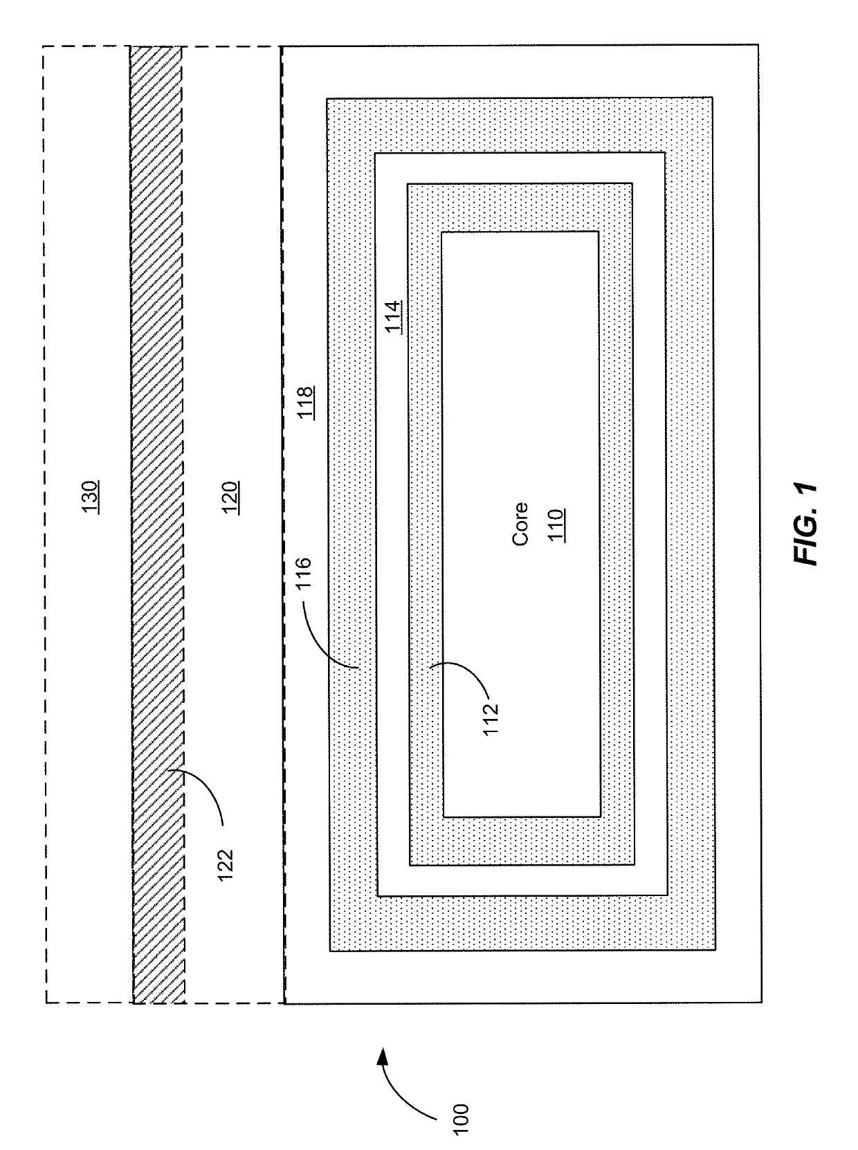
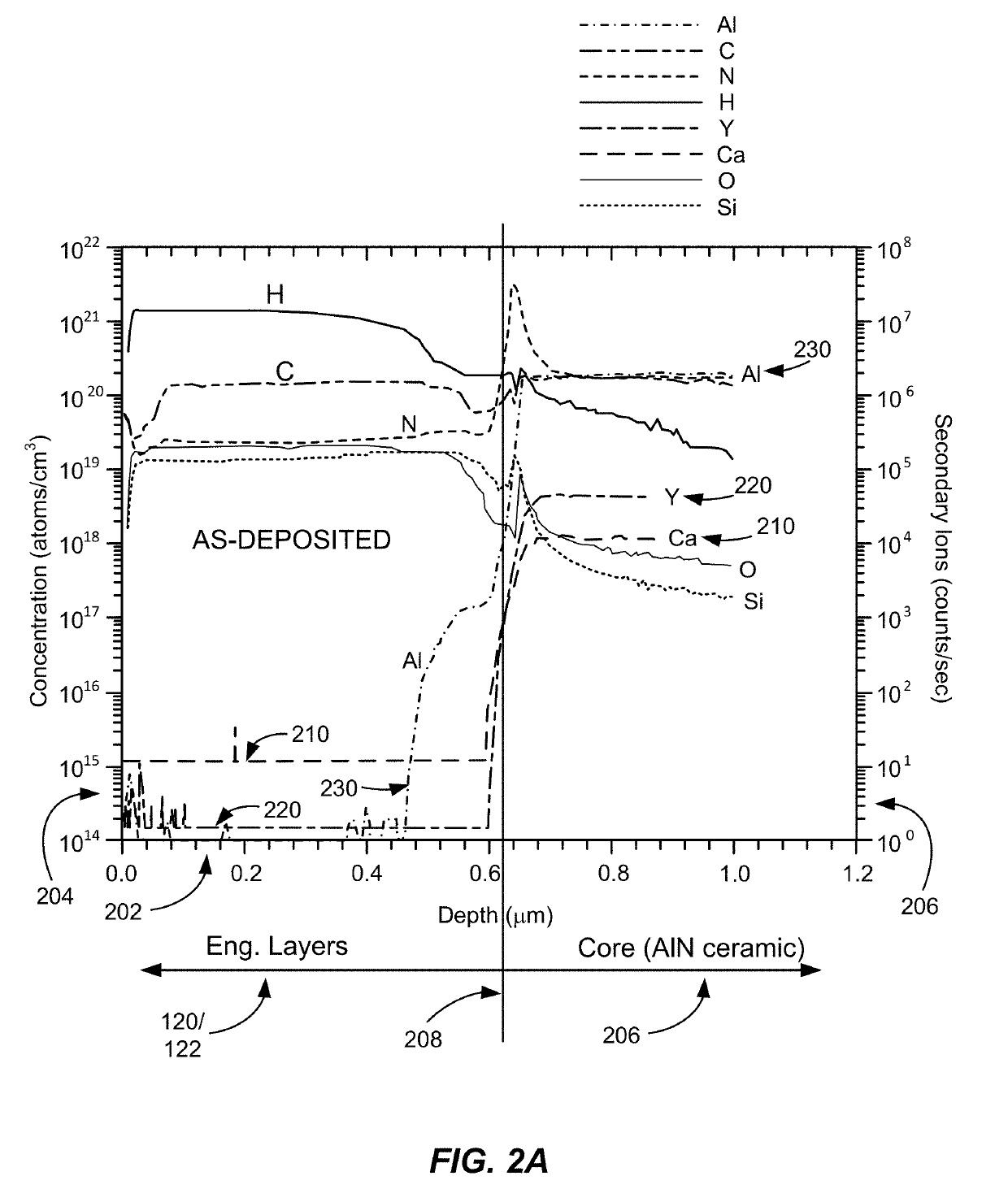
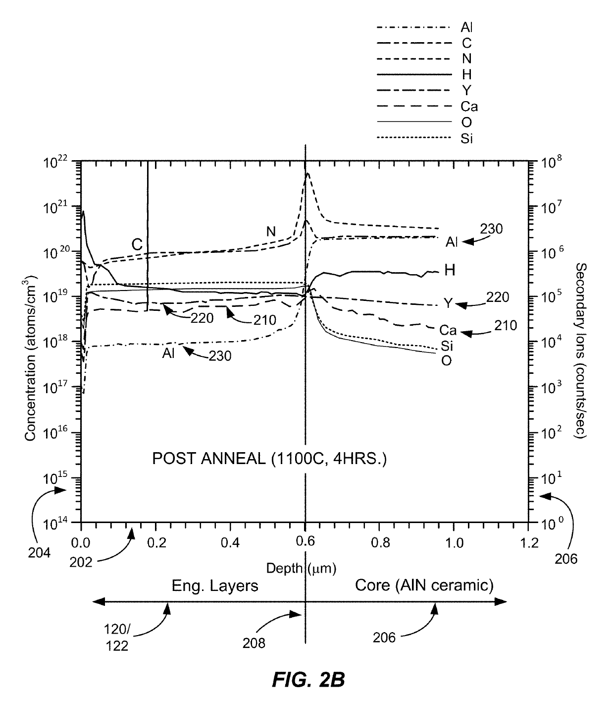
[0026]The present invention relates generally to fabricating an integrated circuit comprising a system of stacked devices using an engineered substrate structure as an interposer. In some embodiments, the engineered substrate structure can be a polycrystalline interposer characterized by a coefficient of thermal expansion (CTE) that is substantially matched to the CTE of devices bonded to the interposer. The use of an interposer versus monolithically integrated devices can reduce the interconnect length, form factor, and overall cost of an integrated circuit. In some embodiments, the reduced interconnect length can result in reduced power consumption and increased bandwidth between the devices. A polycrystalline interposer can be a passive layer. In some embodiments, a polycrystalline interposer with a CTE substantially matched to substrates and devices bonded thereon improves thermal management and stress when compared to existing technologies. Embodiments described herein use an e...


PUM

PropertyMeasurementUnit
diameteraaaaaaaaaa
thicknessaaaaaaaaaa
thicknessaaaaaaaaaa

Abstract

An interposer includes a polycrystalline ceramic core disposed between a first surface and a second surface of the interposer, an adhesion layer encapsulating the polycrystalline ceramic core, a barrier layer encapsulating the adhesion layer, and one or more electrically conductive vias extending from the first surface to the second surface through the polycrystalline ceramic core, the adhesion layer, and the barrier layer.

Description

CROSS-REFERENCES TO RELATED APPLICATIONS[0001]This application claims priority to U.S. Provisional Patent Application No. 62 / 598,355, filed on Dec. 13, 2017, the disclosure of which is hereby incorporated by reference in its entirety for all purposes.BACKGROUND OF THE INVENTION[0002]Heteroepitaxy of gallium nitride based compound semiconductors on sapphire, silicon carbide and silicon is currently used to fabricate devices such as light-emitting diodes (LEDs), high power devices, and high speed radio frequency (RF) devices. Applications include lighting, computer monitors, displays, wide band gap communications, automotive, and industrial power sources. The growth of gallium nitride based devices on a sapphire substrate is a heteroepitaxial growth process since the substrate and the epitaxial layers are composed of different materials. Due to the heteroepitaxial growth process, the epitaxially grown material can exhibit a variety of adverse effects, including reduced uniformity and ...

Claims


Application Information

Patent Timeline
Patent Type & Authority Applications(United States)
IPC IPC(8): H01L25/065H01L23/15H01L23/373H01L23/498H01L21/48H01L25/00
CPCH01L25/0657H01L23/15H01L23/3735H01L23/49827H01L23/49894H01L21/486H01L25/50H01L2225/06517H01L2225/06548H01L2225/06572H01L2225/06589H01L23/5384H01L24/13H01L24/16H01L2224/0401H01L2224/13009H01L2224/131H01L2224/16235H01L2224/81191H01L2225/06541H01L2924/10253H01L2924/14H01L2924/141H01L2924/143H01L2924/1434H01L2924/013H01L2924/00014
Inventor ODNOBLYUDOV, VLADIMIRBASCERI, CEMFARRENS, SHARI
Owner QROMIS INC
Why Eureka
Try Eureka