Polishing apparatus

Active Publication Date: 2019-07-18
EBARA CORP
View PDF4 Cites 0 Cited by
  • Summary
  • Abstract
  • Description
  • Claims
  • Application Information

AI Technical Summary

Benefits of technology

The invention is a polishing apparatus that can accurately measure the thickness of a film on a wafer by regulating the amount of light that illuminates it. The apparatus has two dimmable lights that control the quantity of reflected light from the wafer: a first dimmer controls the overall amount of light, and a second dimmer balances the light directed from different fibers. By adjusting the position of the light source and dimming the light, the apparatus can measure the film thickness at different locations on the wafer with high accuracy. This technology allows for precise control over the polishing process, improving efficiency and accuracy.

Problems solved by technology

Furthermore, if the quantity of reflected light from the wafer is too large relative to an effective measuring range of the spectrometer, measuring of an accurate film thickness is hindered.

Method used


Image

  • Polishing apparatus
  • Polishing apparatus
  • Polishing apparatus

Examples


Embodiment Construction

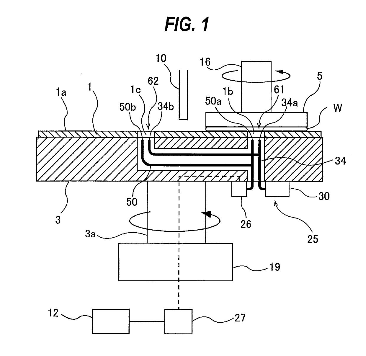
[0039]Embodiments will be described below with reference to the drawings. FIG. 1 is a view showing an embodiment of a polishing apparatus. As shown in FIG. 1, the polishing apparatus includes a polishing table 3 supporting a polishing pad 1, a polishing head 5 for holding a wafer W and pressing the wafer W against the polishing pad 1 on the polishing table 3, a polishing-liquid supply nozzle 10 for supplying a polishing liquid (e.g., slurry) onto the polishing pad 1, and an operation controller 12 for controlling polishing of the wafer W.

[0040]The polishing table 3 is coupled to a table motor 19 through a table shaft 3a, so that the polishing table 3 is rotated by the table motor 19 in a direction indicated by arrow. The table motor 19 is located below the polishing table 3. The polishing pad 1 is attached to an upper surface of the polishing table 3. The polishing pad 1 has an upper surface, which provides a polishing surface 1a for polishing the wafer W. The polishing head 5 is se...


PUM


Abstract

A polishing apparatus capable of accurately measuring a film thickness by regulating a quantity of light illuminating a wafer is disclosed. The polishing apparatus includes: a light source; an illuminating fiber having distal ends arranged at different locations in the polishing table; and a light-receiving fiber having distal ends arranged at the different locations in the polishing table. The illuminating fiber includes a first illuminating fiber and a second illuminating fiber. A first dimmer is attached to the first illuminating fiber and the second illuminating fiber, and a second dimmer is attached to at least one of the first illuminating fiber and the second illuminating fiber.

Description

CROSS REFERENCE TO RELATED APPLICATION[0001]This document claims priority to Japanese Patent Application Number 2018-6358 filed Jan. 18, 2018, the entire contents of which are hereby incorporated by reference.BACKGROUND[0002]Manufacturing processes of semiconductor devices include a process of polishing a dielectric film, e.g., SiO2, and a process of polishing a metal film, e.g., copper or tungsten. Manufacturing processes of backside illumination CMOS sensor and through-silicon via (TSV) include a process of polishing a silicon layer (silicon wafer), in addition to the polishing processes of the dielectric film and the metal film. Polishing of a wafer is terminated when a thickness of a film (e.g., the dielectric film, the metal film, or the silicon layer), constituting a wafer surface, has reached a predetermined target value.[0003]Polishing of a wafer is carried out using a polishing apparatus. In order to measure a film thickness of a non-metal film, such as a dielectric film or...

Claims


Application Information

Patent Timeline
IPC IPC(8): G01B11/06B24B49/12H01L21/67B24B37/005B24B37/34F21V8/00
CPCG01B11/0633B24B49/12H01L21/67092H01L21/67253B24B37/005B24B37/34G02B6/0008G02B6/266G02B6/3506G01B11/0625B24B37/013H01L21/304
Inventor KIMBA, TOSHIFUMITAKAHASHI, NOBUYUKIKINOSHITA, MASAKI
Owner EBARA CORP
Why Eureka
Try Eureka