
Photonic chip with an input wavelength filter

Active Publication Date: 2019-07-25
ELENION TECH LLC
View PDF2 Cites 16 Cited by
  • Summary
  • Abstract
  • Description
  • Claims
  • Application Information

AI Technical Summary

Benefits of technology

The present patent relates to a method and device for blocking or processing light in a photonic chip. The method involves using a port layer and a device layer in the chip, with a two-layer wavelength-selective coupler to connect light from an external source at a first wavelength and block or process the light at a second wavelength. The device layer includes one or more device waveguides and the port layer includes one or more port waveguides. The port waveguides are optically coupled to the device waveguides to form a composite optical port for connecting to the external optical system. The device layer may be a semiconductor layer or an absorptive layer. The patent also relates to a photonic chip that includes a plurality of port layers and a device layer, with the port layers and device layer configured to block or process light at different wavelengths. The technical effects of the patent include improved optical coupling and wavelength selective coupling, as well as improved light blocking and processing capabilities.

Problems solved by technology

This general scheme, although capable of performing its function, requires however a relatively large number of optical components, which increases its cost and size.

Method used


Image

  • Photonic chip with an input wavelength filter
  • Photonic chip with an input wavelength filter
  • Photonic chip with an input wavelength filter

Examples


Embodiment Construction

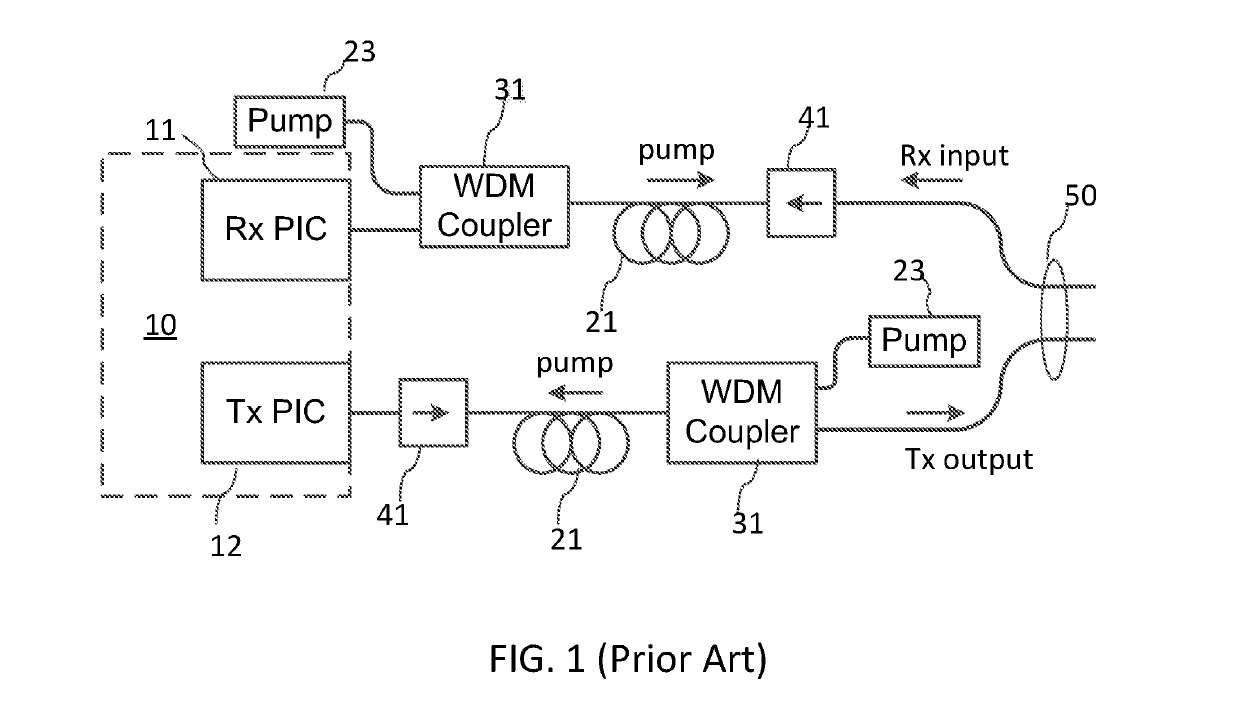
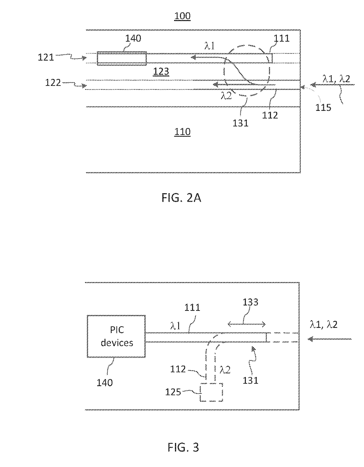
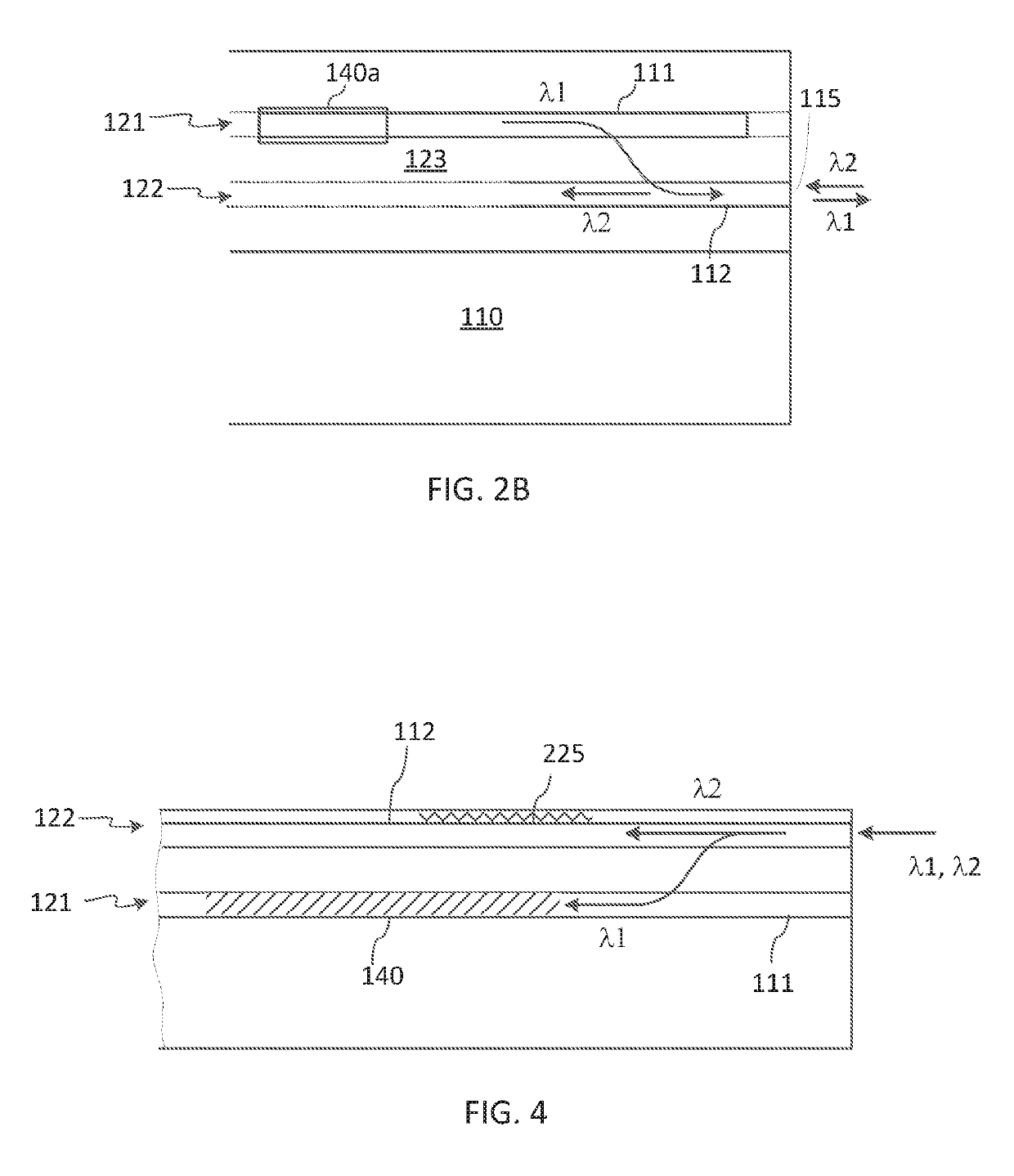
[0032]In the following description, for purposes of explanation and not limitation, specific details are set forth, such as particular optical circuits, circuit components, techniques, etc. in order to provide a thorough understanding of the present invention. However, it will be apparent to one skilled in the art that the present invention may be practiced in other embodiments that depart from these specific details. In other instances, detailed descriptions of well-known methods, devices, and circuits are omitted so as not to obscure the description of the present invention. All statements herein reciting principles, aspects, and embodiments of the invention, as well as specific examples thereof, are intended to encompass both structural and functional equivalents thereof. Additionally, it is intended that such equivalents include both currently known equivalents as well as equivalents developed in the future, i.e., any elements developed that perform the same function, regardless...


PUM


Abstract

A photonic chip includes a device layer and a port layer, with an optical port located at the port layer. Inter-layer optical couplers are provided for coupling light between the device and port layers. The inter-layer couplers may be configured to couple signal light but block pump light or other undesired wavelength from entering the device layer, operating as an input filter. The port layer may accommodate other light pre-processing functions, such as optical power splitting, that are undesirable in the device layer.

Description

FIELD OF THE INVENTION[0001]The invention generally relates to photonic integrated circuits, and more particularly relates to a photonic chip with a two-layer wavelength selective coupler at its optical interface.BACKGROUND OF THE INVENTION[0002]Photonic integrated circuits are widely used in optical communication systems, in particular to implement optical transceivers. An optical transceiver may include an optical transmitter for transmitting optical signals into a fiber optic link, and an optical receiver for receiving optical signals from the fiber optical link. Often the optical link includes an optical amplifier, such as an erbium-doped fiber amplifier (EDFA) in the vicinity of the optical transceiver, which has to be optically pumped by pump light, which may propagate towards the transceiver or away from the transceiver. Typically an optical isolator is required either at the optical link side or at the transceiver side of the EDFA to filter out the pump light. This is illust...

Claims


Application Information

Patent Timeline
IPC IPC(8): G02B6/12G02B6/42H04Q11/00G02B6/27G02B6/122H04B10/43H04J14/02
CPCG02B6/12016G02B6/4215H04Q11/0005G02B6/2773G02B6/4206G02B6/1228H04B10/43H04J14/0278G02B6/12002G02B6/12007G02B6/124G02B6/42H04B10/40H04J14/02
Inventor NOVACK, ARISHI, RUIZHIHORTH, ALEXANDREDING, RANHOCHBERG, MICHAEL J.
Owner ELENION TECH LLC
Features
  • Generate Ideas
  • Intellectual Property
  • Life Sciences
  • Materials
  • Tech Scout
  • Unparalleled Data Quality
  • Higher Quality Content
  • 60% Fewer Hallucinations
Learn More