Wiring substrate for inspection apparatus

a technology of wiring substrate and inspection apparatus, which is applied in the direction of printed circuit stress/warp reduction, semiconductor/solid-state device testing/measurement, instruments, etc., can solve the problems of difficult to form electrically conductive paths with high precision, difficult to provide very narrow spacing, and thick formation of tile substrates, etc., to achieve stable impedance matching and reduce overall size

Active Publication Date: 2019-08-22
NGK SPARK PLUG CO LTD
View PDF3 Cites 0 Cited by
  • Summary
  • Abstract
  • Description
  • Claims
  • Application Information

AI Technical Summary

Benefits of technology

[0006]The present invention has been accomplished so as to solve the problem described in Background Art, and an object of the present invention is to reliably provide a wiring substrate for inspection apparatus having a plurality of tile substrates, each of which can achieve a reduction in overall size, has high-precision electrically conductive paths provided therein, can achieve narrow spacing between surface pads, and realizes stable impedance matching.

Problems solved by technology

However, since the tile substrate is formed of an insulating material, such as ceramic, electrically conductive paths, such as inner wiring layers and via conductors, formed in the tile substrate tend to become thick.
Also, since firing shrinkage in firing ceramic must be considered in providing spacing between surface pads formed on the surface of the tile substrate, difficulty is encountered in providing very narrow spacing.
As a result, difficulty is encountered in forming electrically conductive paths with high precision in the tile substrate, and impedance matching is apt to become unstable.
As a result, there has been a potential failure to conduct high-precision inspection through a plurality of interconnection elements which free-stand on the surface of the tile substrate and come into electrical contact with an electronic component to be inspected.

Method used


Image

  • Wiring substrate for inspection apparatus
  • Wiring substrate for inspection apparatus
  • Wiring substrate for inspection apparatus

Examples


Embodiment Construction

[0040]An embodiment of the present invention will next be described.

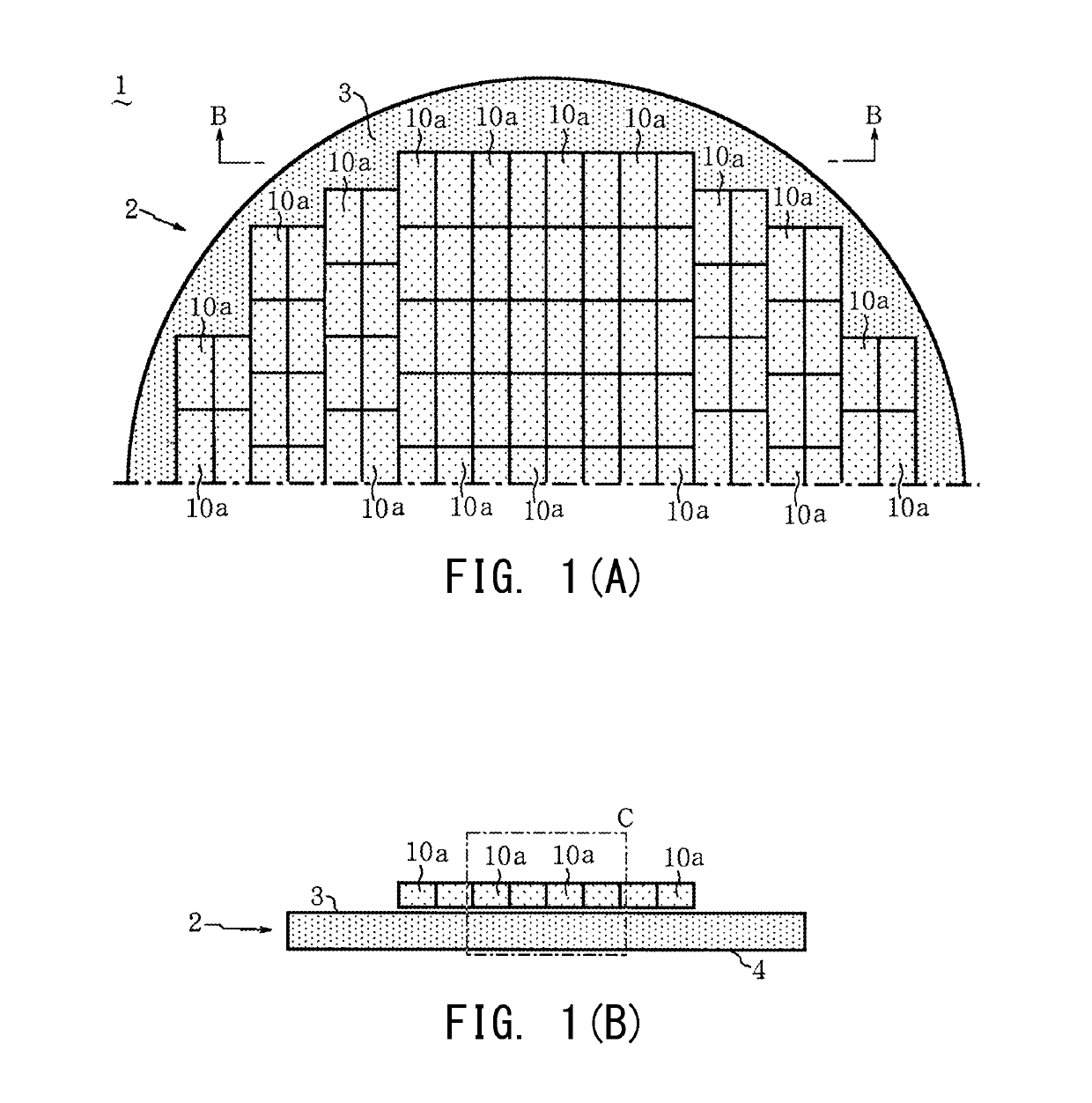
[0041]FIG. 1(A) is a fragmentary plan view showing a wiring substrate for inspection apparatus 1 according to an embodiment of the present invention, and FIG. 1(B) is a fragmentary vertical sectional view taken along line B-B of FIG. 1(A).

[0042]As shown in FIGS. 1(A) and 1(B), the wiring substrate for inspection apparatus (hereinafter, called merely the wiring substrate) 1 includes a disk-shaped base substrate 2 having a base front-surface 3 and a base back-surface 4 having a circular shape in plan view and located on opposite sides of the base substrate 2, and a plurality of tile substrates 10a mounted on the base front-surface 3 of the base substrate 2 adjacent to one another in plan view. Each tile substrate 10a has a rectangular shape in plan view measuring about 10 mm to 15 mm in length of long side and about 5 mm to 7 mm in length of short side.

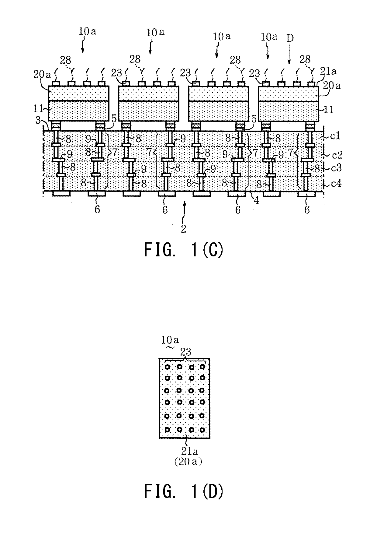
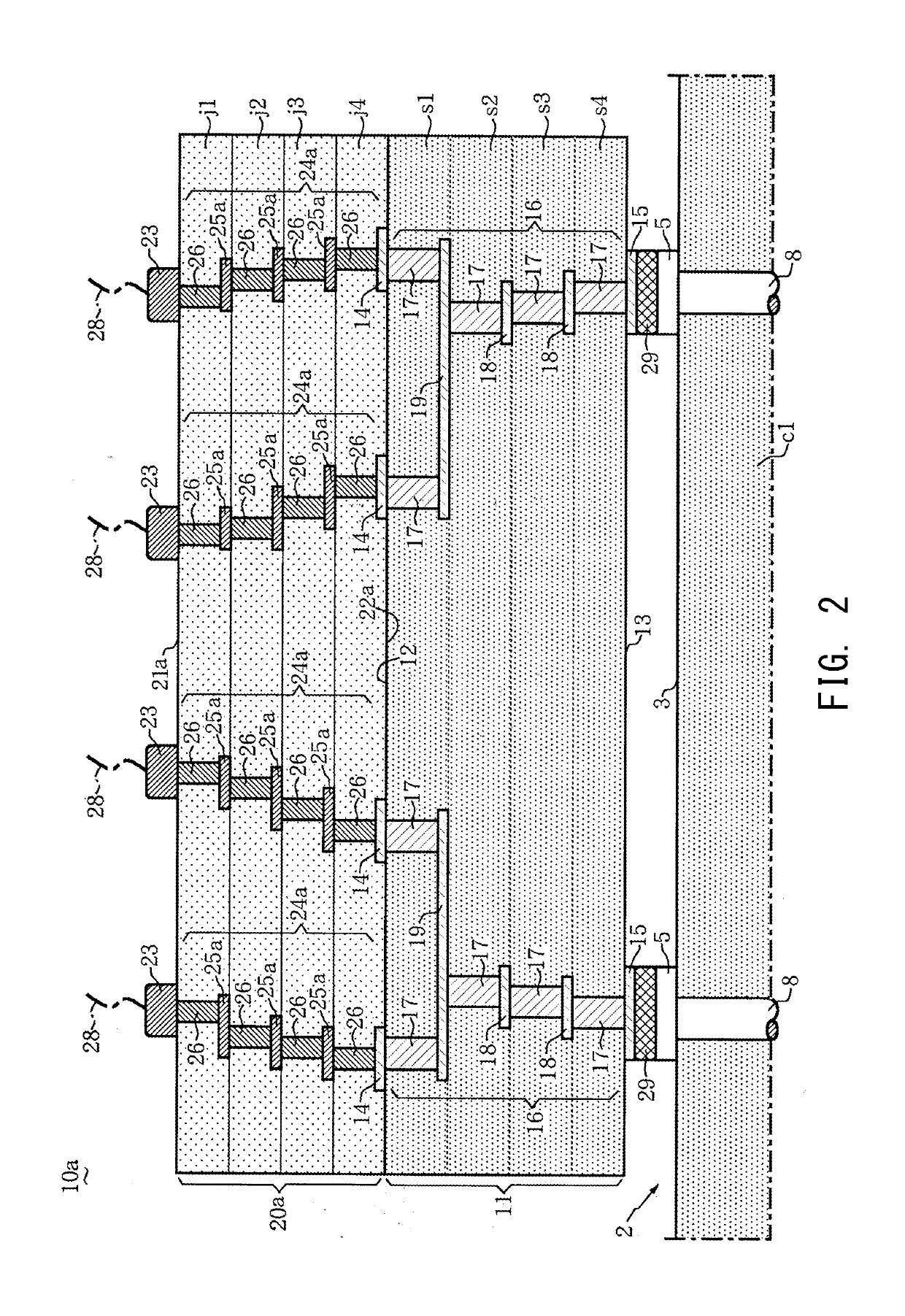
[0043]As shown in FIG. 1(C), the base substrate 2 is a laminate of...


PUM

PropertyMeasurementUnit
diameteraaaaaaaaaa
lengthaaaaaaaaaa
lengthaaaaaaaaaa

Abstract

A wiring substrate for inspection apparatus includes a base substrate and a plurality of tile substrates. The tile substrate is composed of a ceramic substrate section and a first resin substrate section. Each ceramic substrate section is composed of a plurality of ceramic layers and has a plurality of upper-surface connection terminals provided on an upper surface thereof, a plurality of lower-surface connection terminals provided on a lower surface thereof, and a plurality of through conductors for conducting electricity between the upper-surface connection terminals and the lower-surface connection terminals. The first resin substrate section is laminated on the upper surface and includes a laminate of a plurality of resin layers, a plurality of probe pads formed on a resin front-surface thereof, a plurality of inner wiring layers formed between the resin layers, and a plurality of electrically conductive paths for conducting electricity between the probe pads and the upper-surface connection terminals.

Description

CROSS REFERENCE TO RELATED APPLICATION[0001]The present application claims priority to Japanese Patent Application No. 2018-027329, which was filed on Feb. 19, 2018, the disclosure of which is herein incorporated by reference in its entirety.BACKGROUND OF THE INVENTIONField of the Invention[0002]The present invention relates to a wiring substrate for use in an inspection apparatus for individually inspecting electrical characteristics of, for example, a large number of electronic components formed along the surface of a silicon wafer.Description of Related Art[0003]For example, in order to individually inspect electrical characteristics of a large number of electronic components formed along the surface of a silicon wafer having a diameter of about 30 cm, contact carriers (tiles) have been proposed for use in a probe card configured such that a large number of tile substrates individually corresponding to a large number of the electronic components (chips) are mounted on the surface...

Claims


Application Information

Patent Timeline
Patent Type & Authority Applications(United States)
IPC IPC(8): H05K1/14H05K1/11H05K1/03G01R1/073G01R31/28
CPCH05K1/141H05K1/113H05K1/0306H05K1/0346G01R1/07342G01R31/2831H05K2201/0154H05K2201/10378G01R1/07314H01L22/34H05K1/0271H05K3/4061H05K3/429H05K2201/0195H05K2201/041H05K2201/09027H05K2201/096G01R31/2886H05K1/025H05K1/114H05K3/4611H05K3/4629
Inventor NASU, TAKAKUNI
Owner NGK SPARK PLUG CO LTD
Why Eureka
Try Eureka