Multilayer ceramic capacitor and manufacturing method of multilayer ceramic capacitor

a multi-layer ceramic capacitor and manufacturing method technology, applied in the direction of fixed capacitors, stacked capacitors, fixed capacitor details, etc., can solve the problems of uneven thickness of internal electrode layers and degrade reliability, and achieve the effect of reducing the continuity modulus of internal electrodes after sintering and facilitating sintering

Active Publication Date: 2019-08-29
TAIYO YUDEN KK
View PDF0 Cites 20 Cited by
  • Summary
  • Abstract
  • Description
  • Claims
  • Application Information

AI Technical Summary

Benefits of technology

[0004]A continuity modulus of an internal electrode after sintering is reduced because of a difference between a sintering start temperature of a metal of the internal electrode layer and a sintering start temperature of ceramic of a dielectric layer. Therefore, a co-material of ceramic is added to the internal electrode layer in order to delay contraction of the internal electrode layer. However, when a thickness of the internal electrode layer is reduced, the co-material tends to be extruded to the dielectric layer side. Thereby, surface roughness of the internal electrode layer may be enlarged. Therefore, a thickness of the internal electrode layer becomes uneven in a stacking direction of the dielectric layer and the internal electrode layer. When the thickness of the internal electrode layer in uneven, a liquid phase tends to be flocculated in an interface between the internal electrode layer and the dielectric layer in a region of the internal electrode layer of which a thickness is small. And reliability may be degraded.

Problems solved by technology

Therefore, a thickness of the internal electrode layer becomes uneven in a stacking direction of the dielectric layer and the internal electrode layer.
And reliability may be degraded.

Method used


Image

  • Multilayer ceramic capacitor and manufacturing method of multilayer ceramic capacitor
  • Multilayer ceramic capacitor and manufacturing method of multilayer ceramic capacitor
  • Multilayer ceramic capacitor and manufacturing method of multilayer ceramic capacitor

Examples


embodiment

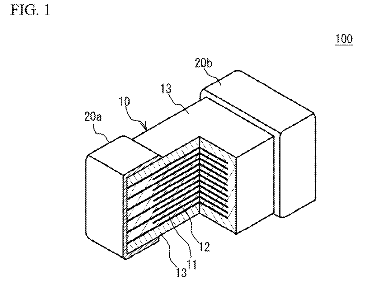
[0017]FIG. 1 illustrates a partial perspective view of a multilayer ceramic capacitor 100 in accordance with an embodiment. As illustrated in FIG. 1, the multilayer ceramic capacitor 100 includes a multilayer chip 10 having a rectangular parallelepiped shape, and a pair of external electrodes 20a and 20b that are respectively provided at two edge faces of the multilayer chip 10 facing each other. In four faces other than the two edge faces of the multilayer chip 10, two faces other than an upper face and a lower face of the multilayer chip 10 in a stacking direction are referred to as side faces. The external electrodes 20a and 20b extend to the upper face, the lower face and the two side faces. However, the external electrodes 20a and 20b are spaced from each other.

[0018]The multilayer chip 10 has a structure designed to have dielectric layers 11 and internal electrode layers 12 alternately stacked. A main component of the dielectric layer 11 is a ceramic material acting as a diele...

examples

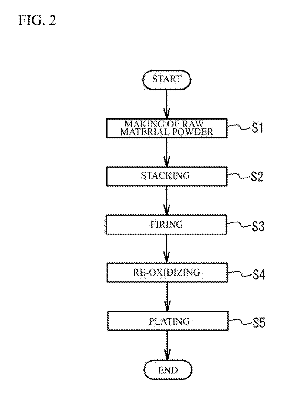
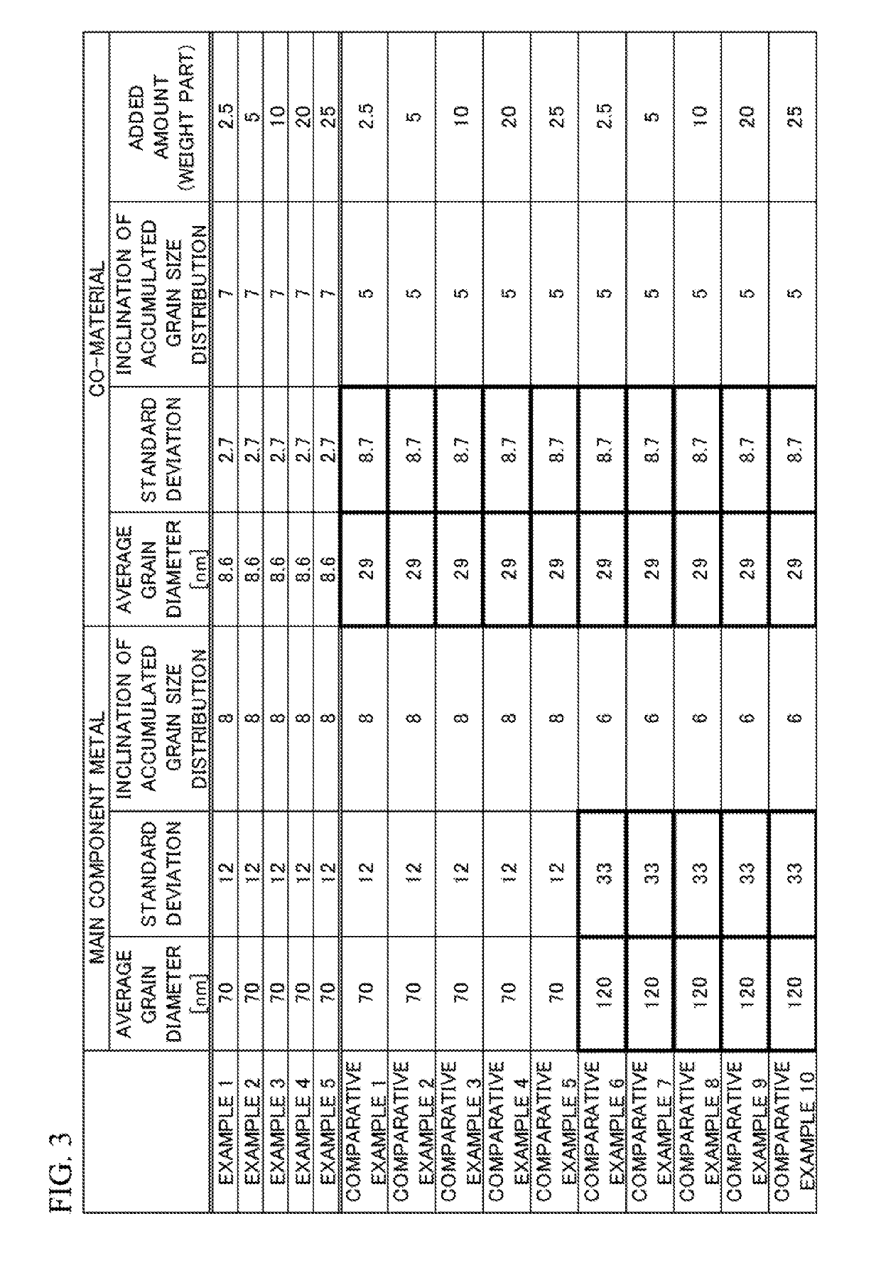
[0035]The multilayer ceramic capacitors in accordance with the embodiment were made and the property was measured.

[0036](Examples 1 to 5) A necessary additive compound was added to barium titanate powder of which an average grain diameter was 100 nm (a specific surface area of 10 m2 / g). The resulting barium titanate powder was sufficiently wet-blended and crushed with a ball mil. Thus, the dielectric material was obtained. An organic binder and a solvent were added to the dielectric material. And dielectric green sheets were made by a doctor blade method. A thickness of the dielectric green sheet was 0.8 μm. The organic binder was polyvinyl butyral (PVB) resin or the like. The solvent was ethanol, toluene or the like. And a plasticizer and so on were added.

[0037]Next, the conductive paste for forming the internal electrode layer was formed by a planetary boll mill. The conductive paste included a main component metal (Ni) powder of the internal electrode layer 12 (50 wt % of Ni soli...


PUM

PropertyMeasurementUnit
arithmetic average roughnessaaaaaaaaaa
height Rzaaaaaaaaaa
arithmetic average roughnessaaaaaaaaaa

Abstract

A multilayer ceramic capacitor includes: a multilayer structure in which each of a plurality of dielectric layers and each of a plurality of internal electrode layers are alternately stacked, a main component of the dielectric layers being ceramic, a main component of the internal electrode layer being a metal, wherein an arithmetic average roughness Ra of at least a part of the internal electrode layer is 30 nm or less, wherein a maximum height Rz of the at least a part of the internal electrode layer is 360 nm or less.

Description

CROSS-REFERENCE TO RELATED APPLICATION[0001]This application is based upon and claims the benefit of priority of the prior Japanese Patent Application No. 2018-031512, filed on Feb. 26, 2018, the entire contents of which are incorporated herein by reference.FIELD[0002]A certain aspect of the present invention relates to a multilayer ceramic capacitor and a manufacturing method of a multilayer ceramic capacitor.BACKGROUND[0003]Recently, electronic devices such as smart phones or mobile phones are being downsized. Thereby, electronic components mounted on the electronic devices are rapidly being downsized. For example, in a field of multilayer ceramic capacitors, although property is secured, thicknesses of dielectric layers and internal electrode layers are reduced in order to reduce a chip size (for example, see Japanese Patent Application Publication No. 2014-57098).SUMMARY OF THE INVENTION[0004]A continuity modulus of an internal electrode after sintering is reduced because of a d...

Claims


Application Information

Patent Timeline
Patent Type & Authority Applications(United States)
IPC IPC(8): H01G4/012H01G4/008H01G4/12H01G4/30
CPCH01G4/012H01G4/30H01G4/1227H01G4/0085H01G4/008
Inventor MAKINO, TORU
Owner TAIYO YUDEN KK
Why Eureka
Try Eureka