Dual voltage and current loop linearization control and voltage balancing control for solid state transformer

a voltage balancing control and solid-state transformer technology, applied in the direction of power electronics conversion, power conversion systems, electrical apparatuses, etc., can solve the problems of grid current being slightly distorted, requiring significant amount of reactive current flow, over-voltage protection, etc., to minimize the enhance the voltage balancing control of chb modules, and minimize the effect of hv side dc bus voltage unbalan

Active Publication Date: 2019-10-10
NANYANG TECH UNIV
View PDF0 Cites 20 Cited by
  • Summary
  • Abstract
  • Description
  • Claims
  • Application Information

AI Technical Summary

Benefits of technology

[0013]The above and other problems are solved and an advance in the state of the art is made by systems and methods provided by embodiments in accordance with the disclosure. The first advantage of embodiments of systems and methods in accordance with the disclosure is that systems and methods are able to minimize the HV side DC bus voltage unbalance in SST start-up process with enforced reactive current flow in CHB converter circuit with enhanced CHB module voltage balancing control implemented. The second advantage of embodiments of systems and methods in accordance with the disclosure is that systems and methods are able to minimize the HV side DC bus voltage unbalance in S

Problems solved by technology

The unbalanced HV side DC bus voltage will cause the capacitor or power device overvoltage in the CHB and DAB circuit and trigger the SST overvoltage protection.
The often cited limitation of this type of voltage balancing solution is that it requires significant amount of reactive current flow in the CHB converter for the voltage balancing algorithm to work properly in light load condition.
Another disadvantage of CHB voltage balancing algorithm is that the grid current is slightly distorted due to PWM modulation signal injection from the voltage balancing algorithm.
The disadvantage of the power balancing control scheme based on that shown in FIGS. 3a and 3b is that the CHB voltage balancing control is only applied as inputs to the d-axis voltages.
This type of voltage balancing control is not effective in the start-up process of SST when only CHB converter control is activated and when CHB is operating around zero power condition.
For this power balancing control scheme, reactive curr

Method used


Image

  • Dual voltage and current loop linearization control and voltage balancing control for solid state transformer
  • Dual voltage and current loop linearization control and voltage balancing control for solid state transformer
  • Dual voltage and current loop linearization control and voltage balancing control for solid state transformer

Examples


first embodiment

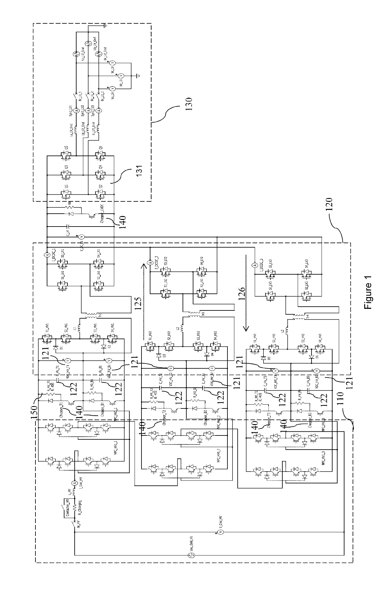
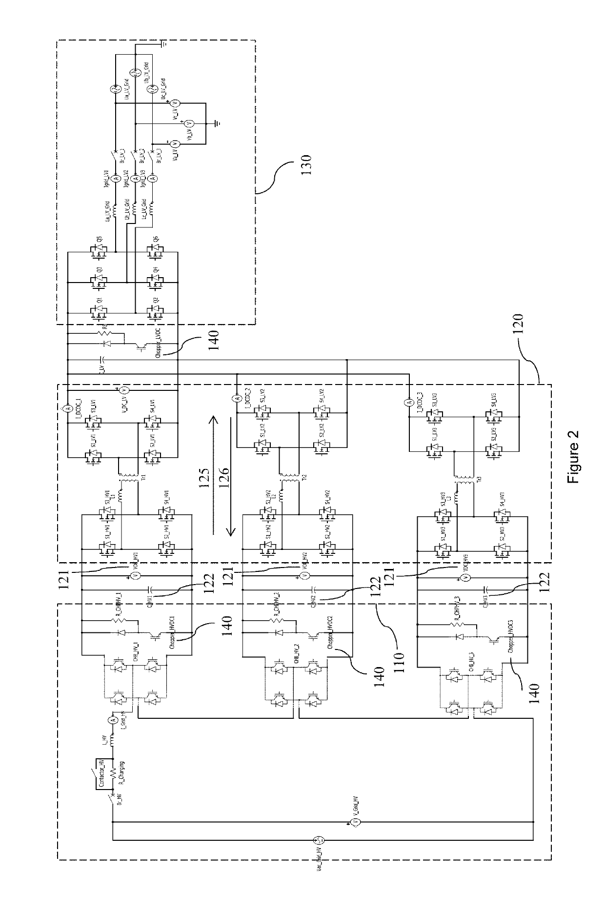
[0080]The method and system according to the DAB current distribution with a dual current and voltage loop voltage balancing control is capable of achieving excellent voltage balancing performance in the zero power or light load condition without requiring HV grid current flow and robust to SST CHB and DAB circuit parameter variations. The combination of CHB voltage balancing control with minimum reactive power / current injection at SST start-up process and DAB voltage balancing control in normal SST power regulation is the best SST voltage balancing scheme to minimise the capacitor voltage variation in HV DC bus.

[0081]The DAB current distribution with a dual current and voltage loop voltage balancing control minimizes the HV side DC bus capacitor voltage unbalance in SST start-up process with enforced reactive current flow in CHB converter circuit with enhanced CHB module voltage balancing control implemented. The DAB current distribution with a dual current and voltage loop voltage...

second embodiment

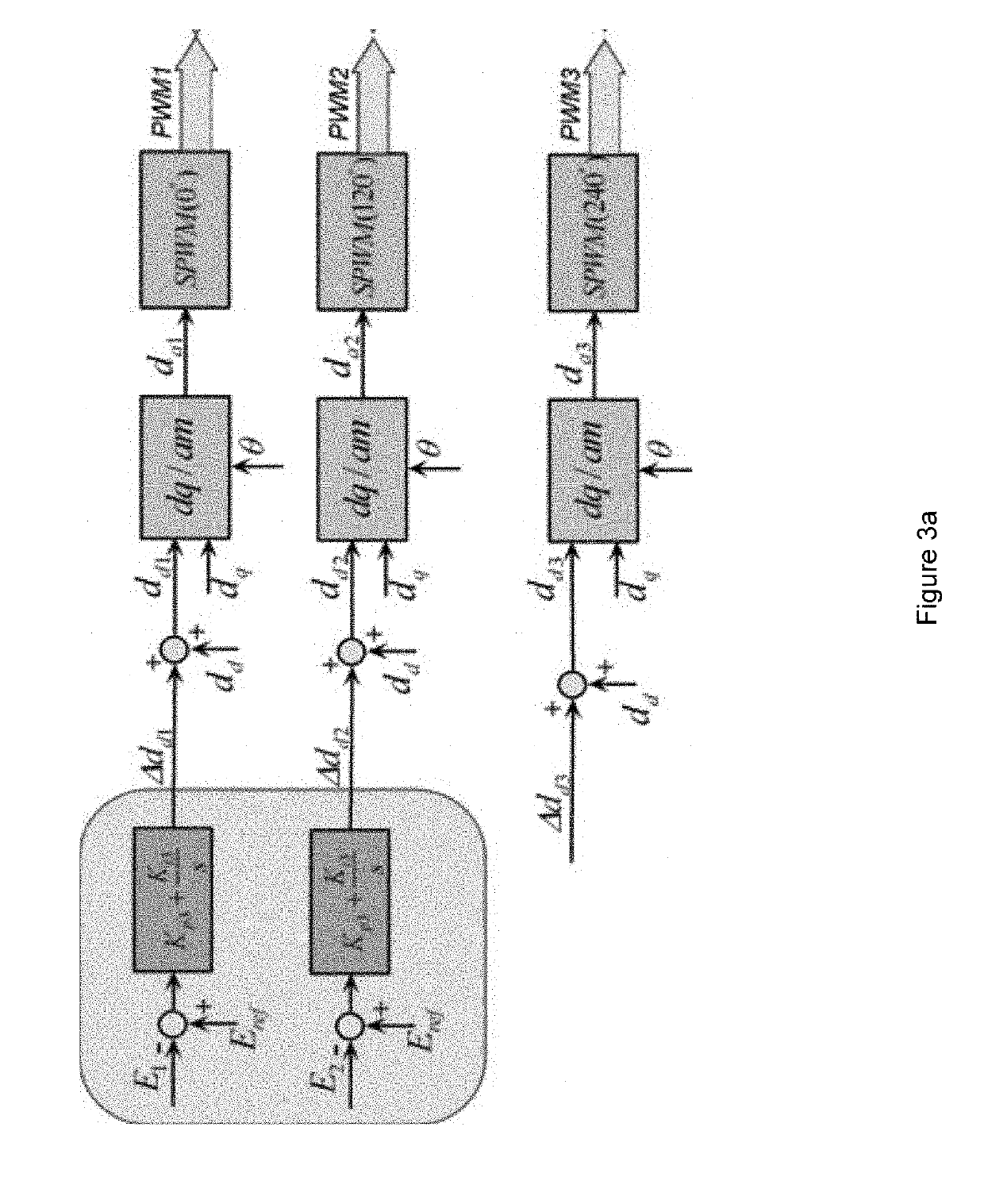
[0121]The method and system according to the second embodiment is that the DAB converter system voltage loop and current control loop are both linearized with non-linear gain compensation so that the conventional linear controller design method can be readily applied in voltage and current controller design to ensure uniformed dynamic performance achieved in all operation conditions.

[0122]The linearized DAB feedback control enables uniformed inner current control loop performance for all DAB modules in SST system with respect to the high frequency transformer parameter variation, the DAB circuit external inductance variation, and HV side DC voltage variation. It also ensures inner current loop has desired stability margins when operates at different inner phase shift angle settings and different HV / LV side DC bus voltage levels. The linearized DAB feedback control achieves uniformed inner current control loop dynamic performance in various operation conditions.

[0123]The outer DAB vo...

third embodiment

[0158]FIG. 25 shows the overview of the third embodiment comprising the DAB current distribution with a dual current and voltage loop voltage balancing control of the first embodiment 2510 and the modular DAB linearized dual voltage and current loop control of the second embodiment2520. The objective of the voltage balancing control is to generate the DAB module current adjustment signals to minimize HV side DC bus voltage unbalance caused by HV side CHB circuit parameter variation, DAB circuit parameter variation, and HF transformer parameter variations. The major advantage of DAB module current distribution based HV bus voltage balancing control is its fast dynamic response which comes from the uniformed inner DAB current loop fast dynamic response for multiple phase shift angle setting changes in full operation range of DAB. Although the first and second embodiments can be individually implemented, it would be advantageous to combine both first and second embodiments to achieve b...


PUM


Abstract

This invention relates to a method of controlling a Solid State Transformer (SST). The method comprises dividing a dual active bridge (DAB) power reference on a Low Voltage (LV) side Direct Current (DC) link voltage to obtain a total DAB reference current; dividing the total DAB current reference by N number of DAB modules to obtain a reference current for each DAB module; in response to SST being in a normal power regulation, determining a deviation of a capacitor voltage at the HV side of each of a k DAB modules with reference from an average voltage from the HV DC bus; determining a current adjustment signal for each of the k DAB modules based on the total DAB reference current and a corresponding deviation of the capacitor voltage of each of the k DAB modules; adding a saturated current adjustment signal together with the reference current for each of the k DAB modules to obtain a total current reference for each of the k DAB modules; and subtracting a sum of the total current reference of each of the k DAB modules from the total DAB reference current to determine a total current reference for an Nth DAB module.

Description

CROSS-REFERENCE TO RELATED APPLICATION[0001]This application claims the benefit of Singapore Patent Application No. 10201802869Q, entitled “Dual Voltage And Current Loop Linearization Control And Voltage Balancing Control For Solid State Transformer” and filed on 5 Apr. 2018, which is expressly incorporated by reference herein in its entirety.Field of the Invention[0002]This disclosure relates to an improved Solid State Transformer (SST). Particularly, this disclosure relates to a Direct Current (DC) bus capacitor voltage balancing method at the High Voltage (HV) side of a SST system. Further, this disclosure relates to a linearized Dual Active Bridge (DAB) feedback control.Background[0003]FIG. 1 shows one known implementation of a modular SST circuit topology for Low Voltage (LV) side grid tied application. Briefly, a SST typically comprises a HV side 110, a LV side 130 and a DAB 120 between the HV 110 and LV 130. Returning back to FIG. 1, the HV side 110 Neutral Point Clamp (NPC) ...

Claims


Application Information

Patent Timeline
IPC IPC(8): H02M5/458H02M1/088
CPCH02M2001/0003H02M5/4585H02M1/088H02M2001/0093H02M1/36H02M5/458H02M1/0032H02M1/007Y02B70/10H02M1/0003H02M1/0093
Inventor CAO, SHUYUVAISAMBHAYANA, BRIHADEESWARA SRIRAMTRIPATHI, ANSHUMANCUI, FENGJIAOSETHUPANDI, ABISHEKDEHGHANI TAFTI, HOSSEIN
Owner NANYANG TECH UNIV
Why Eureka
Try Eureka