Zero cross detection circuit and sensor device

Active Publication Date: 2019-10-24
ABLIC INC
View PDF3 Cites 0 Cited by
  • Summary
  • Abstract
  • Description
  • Claims
  • Application Information

AI Technical Summary

Benefits of technology

[0011]The zero cross detection circuit of the present invention has the power supply voltage detection circuit providing a power supply voltage detection signal to the logic circuit when

Problems solved by technology

The conventional zero cross detection ci

Method used


Image

  • Zero cross detection circuit and sensor device
  • Zero cross detection circuit and sensor device
  • Zero cross detection circuit and sensor device

Examples


Example

First Embodiment

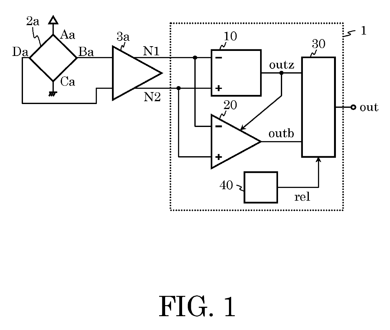
[0025]FIG. 1 is a block diagram illustrating a sensor device having a zero cross detection circuit according to the first embodiment of the present invention. The sensor device according to the first embodiment has a zero cross detection circuit 1, a hall element 2a, and a differential amplifier 3a.

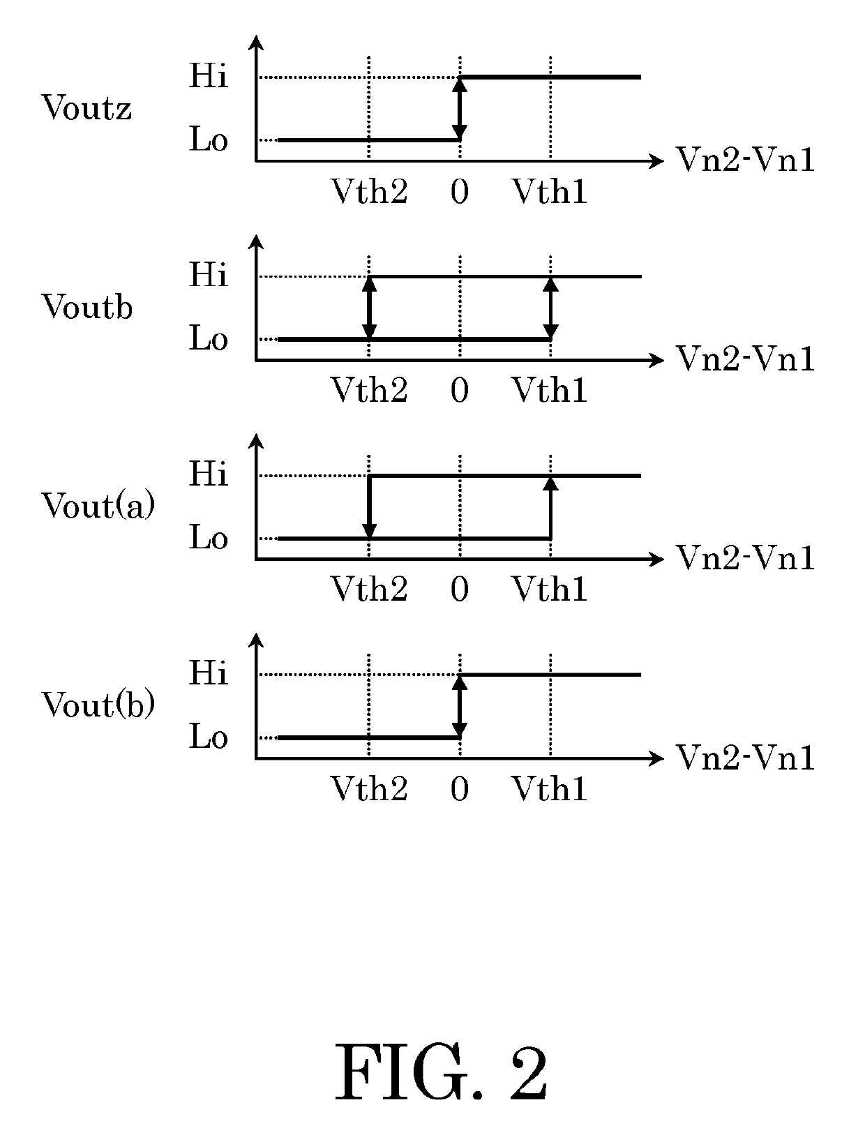
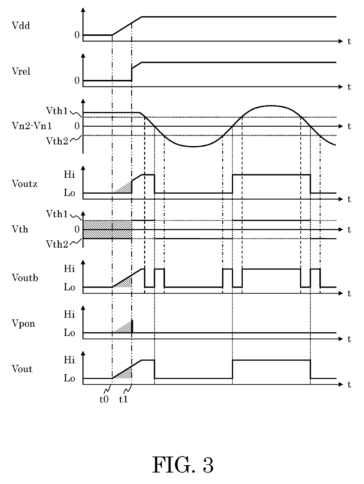
[0026]The zero cross detection circuit 1 has a zero-crossing signal generation circuit 10, a comparator circuit 20, a logic circuit 30, and a power supply voltage detection circuit 40. The zero-crossing signal generation circuit 10 includes a comparator circuit as explained later and has an inverted input terminal, a non-inverted input terminal, and an output terminal outz. The comparator circuit 20 has an inverted input terminal, a non-inverted input terminal, a threshold voltage selection terminal, and an output terminal outb. The non-inverted input terminal of the zero-crossing signal generation circuit 10 and the non-inverted input terminal of the comparator circuit 2...

Example

Second Embodiment

[0068]FIG. 10 is a block diagram illustrating a zero cross detection circuit according to a second embodiment of the present invention. The difference between the zero cross detection circuit 1b illustrated in FIG. 10 and the zero cross detection circuit 1 illustrated in FIG. 1 is that the zero-crossing signal generation circuit 10 is deleted, the comparator circuit 101 in the zero-crossing signal generation circuit 10 is added, the logic circuit 30 is deleted, and a logic circuit 31 is added.

[0069]The added elements are constituted and connected as follows. Moreover, due to the deleted elements, the following connection and operation are different from those of the zero cross detection circuit 1 illustrated in FIG. 1. As in the case of FIG. 1 and FIG. 7, the inverted input terminal of the comparator circuit 101 is connected to the terminal N1 and the non-inverted input terminal is connected in common with the terminal N2. Unlike the case of FIG. 1 and FIG. 7, the o...

Example

Third Embodiment

[0073]FIG. 11 is a block diagram illustrating a magnetic sensor device having the zero cross detection circuit according to the third embodiment of the present invention.

[0074]The configuration of the connection between a hall element 2b and a differential amplifier 3b is the same as the configuration of the connection between the hall element 2a and the differential amplifier 3a of the magnetic sensor device illustrated in FIG. 1. Moreover, the configuration of the connection between a hall element 2c and a differential amplifier 3c is also the same as the configuration of the connection between the hall element 2a and the differential amplifier 3a illustrated in FIG. 1. While the differential amplifier 3a provides differential output, the differential amplifiers 3b and 3c provide single-ended output. A signal from the hall element 2b which is a magnetoelectric transducer is supplied to the differential amplifier 3b from a terminal Bb and a terminal Db, and the diff...


PUM


Abstract

A zero cross detection circuit has a first comparator circuit receiving a first input signal and a second input signal and outputting a first comparison result, a second comparator circuit having a hysteresis function, receiving the first input signal and the second input signal, and outputting a second comparison result, a power supply voltage detection circuit outputting a detection signal when a power supply voltage to be supplied becomes equal to or larger than a predetermined voltage, and a logic circuit outputting a zero cross detection signal based on the first comparison result, the second comparison result, and the detection signal.

Description

RELATED APPLICATIONS[0001]This application claims priority under 35 U.S.C. § 119 to Japanese Patent Application No. 2018-083377 filed on Apr. 24, 2018, the entire content of which is hereby incorporated by reference.BACKGROUND OF THE INVENTION1. Field of the Invention[0002]The present invention relates to a zero cross detection circuit and a sensor device.2. Description of the Related Art[0003]Heretofore, technical measures for preventing noise of an input signal in the vicinity of zero crossing in a zero cross detection circuit has been studied.[0004]FIG. 12 illustrates a conventional zero cross detection circuit. The conventional zero cross detection circuit has a comparator circuit 90, a comparator circuit 91 having a hysteresis, and a logic circuit 92. The comparator circuit 90 provides a zero cross detection result of an input signal nx1 and an input signal nx2 as a voltage Vout90 to an output terminal out90. The comparator circuit 91 provides a comparison result of the input s...

Claims


Application Information

Patent Timeline
IPC IPC(8): G01R19/175G01D5/14
CPCG01R19/175G01D5/14G01R31/343G01R19/16576G01R33/07G01R19/0023
Inventor ARIYAMA, MINORUOKA, TOMOHIROEZAWA, YUSUKE
Owner ABLIC INC
Why Eureka
Try Eureka