Silicon carbide semiconductor device, power converter, and method of manufacturing silicon carbide semiconductor device

a technology of silicon carbide and semiconductor devices, which is applied in the direction of semiconductor devices, electrical devices, transistors, etc., can solve the problems of increasing the on resistance of the mosfet, causing more damage, and reducing the occurrence of insulation breakdown. , to achieve the effect of reducing the occurrence of insulation breakdown

Inactive Publication Date: 2019-11-14
MITSUBISHI ELECTRIC CORP
View PDF0 Cites 11 Cited by
  • Summary
  • Abstract
  • Description
  • Claims
  • Application Information

AI Technical Summary

Benefits of technology

[0007]The present invention has been made to solve the foregoing problem. It is an object of the present invention to provide a silicon carbide semiconductor device capable of reducing the occurrence of insulation breakdown in a gate insulating film to be caused by application of a high electric field to a gate trench resulting from steep voltage variations in an electric field relaxation region.

Problems solved by technology

A high resistance value in a range from the electric field relaxation region to a source electrode is known to develop a tendency to cause breakdown more easily.
This unfortunately increases the ON resistance of the MOSFET.
In this case, the foregoing problem is likely to become more serious.

Method used


Image

  • Silicon carbide semiconductor device, power converter, and method of manufacturing silicon carbide semiconductor device
  • Silicon carbide semiconductor device, power converter, and method of manufacturing silicon carbide semiconductor device
  • Silicon carbide semiconductor device, power converter, and method of manufacturing silicon carbide semiconductor device

Examples


first preferred embodiment

[0034](Configuration)

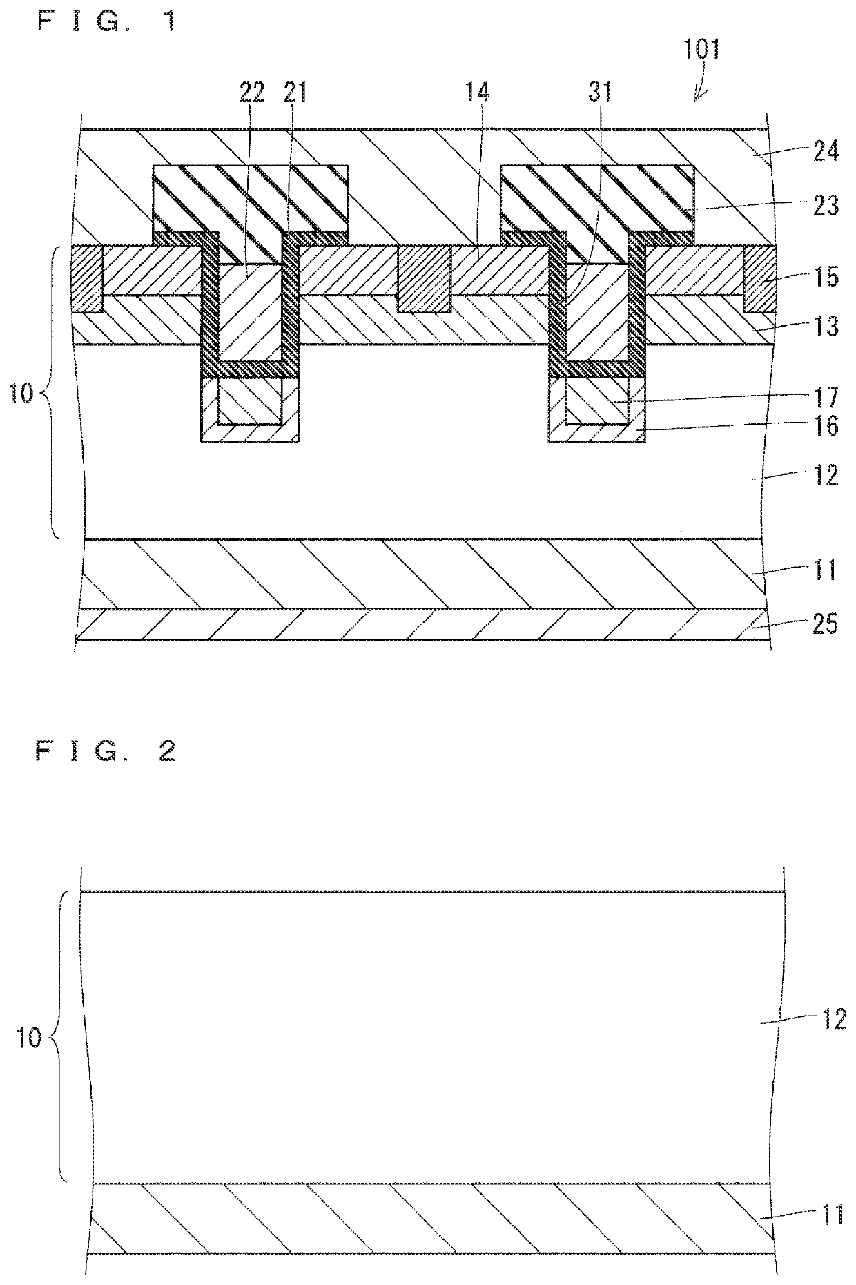
[0035]FIG. 1 is a partial sectional view schematically showing the configuration of an MOSFET 101 (silicon carbide semiconductor device) according to a first preferred embodiment. The MOSFET 101 includes an SiC substrate 11 (silicon carbide substrate), an epitaxial layer 10 (semiconductor layer) provided on one surface (in FIG. 1, upper surface) of the SiC substrate 11, a gate insulating film 21, a gate electrode 22, an interlayer insulating film 23, a source electrode 24, and a drain electrode 25. The epitaxial layer 10 includes a drift layer 12, a well region 13, a source region 14, a well contact region 15, an electric field relaxation region 16, and a surge relaxation region 17. The epitaxial layer 10 is preferably made of SiC.

[0036]In the first preferred embodiment, the SiC substrate 11 has the same conductivity type as the drift layer 12. The drift layer 12 has an n-type (first conductivity type) and is provided on the SiC substrate 11. The drift layer 12 ...

second preferred embodiment

[0068]FIG. 11 schematically shows the configuration of an MOSFET 103 (silicon carbide semiconductor device) according to a second preferred embodiment and is a partial sectional view taken along a line XI-XI in FIG. 12. FIG. 12 is a partial sectional view taken along a line XII-XII in FIG. 11. The illustration of the source electrode 24 is omitted from FIG. 11.

[0069]Referring to FIG. 11, in the second preferred embodiment, multiple cell structures of the MOSFET 103 are aligned in an in-plane direction. In FIG. 11, the gate electrode 22 has a lattice pattern in a planar layout. However, this is not the only planar layout of the gate electrode 22 but the gate electrode 22 may also have a stripe pattern, example.

[0070]Referring to FIG. 12, the right region and the left region in FIG. 12 have configurations similar to the configuration in FIG. 1 (first preferred embodiment). Meanwhile, in the central part of FIG. 12, a source trench 32 is provided in the epitaxial layer 10.

[0071]The sou...

third preferred embodiment

[0077](Configuration)

[0078]FIG. 13 schematically shows the configuration of an MOSFET 104 (silicon carbide semiconductor device) according to a third preferred embodiment and is a partial sectional view taken along a line XIII-XIII in each of FIGS. 14 and 15. FIGS. 14 and 15 are partial sectional views taken along a line XIV-XIV and a line XV-XV respectively in FIG. 13.

[0079]Referring to FIG. 13, in the third preferred embodiment, multiple cell structures of the MOSFET 104 are aligned in an in-plane direction. In FIG. 13, the planar layout of the gate electrode 22, in other words, the planar layout of the gate trench 31 is a stripe pattern.

[0080]Referring to FIG. 14, the MOSFET 104 includes a part where a cross-sectional configuration is similar to the cross-sectional configuration of the MOSFET 101 (FIG. 1). At least this part has the function of forming a channel in the MOSFET 104.

[0081]Referring to FIG. 15, the MOSFET 104 includes a part where a cross-sectional configuration diff...


PUM


Abstract

A drift layer has a first conductivity type and is provided on a silicon carbide substrate. A well region has a second conductivity type and is provided on the drift layer. A source region has the first conductivity type and is provided on the well region. A gate trench has an inner surface with a bottom located at a deeper position than the well region and a lateral part continuous with the bottom. An electric field relaxation region has the second conductivity type and has at least a part located below the bottom of the gate trench. A surge relaxation region has the first conductivity type, contacts at least a part of the bottom of the gate trench, and is separated from the drift layer by the electric field relaxation region.

Description

FIELD OF THE INVENTION[0001]The present relates to a silicon carbide semiconductor device, a power converter, and a method of manufacturing a silicon carbide semiconductor device.BACKGROUND ART[0002]For energy saving of power electronic equipment such as an inverter, loss reduction is required in a semiconductor switching element such as an insulated gate bipolar transistor (IGBT) or a metal oxide semiconductor field effect transistor (MOSFET). The loss is determined by conduction loss and switching loss in the element. To reduce these loses, development is proceeding in technology using a wide bandgap semiconductor material such as silicon carbide (SiC) or gallium nitride (GaN). To reduce loss in an MOSFET, a trench gate MOSFET including a trench for a gate structure, namely, including a gate trench is used.[0003]As stated in International Patent Application Publication No. 2014 / 115280, for example, in a trench gate SiC-MOSFET having an n-type drift layer, a p-type electric field r...

Claims


Application Information

Patent Timeline
Patent Type & Authority Applications(United States)
IPC IPC(8): H01L29/66H01L29/10H01L29/78H01L21/265H01L21/311
CPCH01L29/7813H01L29/66568H01L21/31105H01L29/66712H01L21/2652H01L29/1095H01L29/0611H01L29/0619H01L29/78H01L29/4236H01L29/66477H01L29/0623H01L29/66068H01L29/1608H01L29/0696H01L29/41766H01L29/0865H01L29/0869H01L21/047H01L29/7397
Inventor EBIIKE, YUJIKAGAWA, YASUHIRO
Owner MITSUBISHI ELECTRIC CORP
Why Eureka
Try Eureka