Multilayer circuit board filter

a multi-layer circuit board and filter technology, applied in the field of filters, can solve the problems of increasing the required circuit board area, increasing electric resistance, and efficiency drop, and achieve the effects of increasing electric resistance, efficiency drop, and parasitic inductan

Active Publication Date: 2019-11-28
PANASONIC INTELLECTUAL PROPERTY MANAGEMENT CO LTD
View PDF0 Cites 0 Cited by
  • Summary
  • Abstract
  • Description
  • Claims
  • Application Information

AI Technical Summary

Benefits of technology

[0007]A value of the parasitic inductance is, for example, stated by the following formula in PCT International Patent Application Publication No. WO2015-162656 expressing the inductance of the wiring conductors.
[0008]Lp indicates the length of the conductor, Wp the width of the conductor, and Hp the thickness of the conductor.
[0009]Since ln{2Lp / (Wp+Hp)} is the dominant portion in the formula, the parasitic inductance can be increased by making the wiring conductors long and narrow. Making the wiring conductors narrower, however, increases electric resistance and causes a drop in efficiency. Making the wiring conductors longer also means increasing the required circuit board area.
[0010]In view of the above problem, the present disclosure aims to provide a multilayer circuit board filter that more effectively uses the parasitic inductors of the vias and can be formed with a small required circuit board area.
[0011]In order to solve the above problem, a multilayer circuit board filter according to an aspect of the present disclosure includes an input terminal that extends from a front surface to a rear surface of a multilayer circuit board having at least two wiring layers; a first wiring conductor having an end connected to the input terminal on the rear surface of the multilayer circuit board; a first via that extends from an other end of the first wiring conductor to the front surface of the multilayer circuit board; a second wiring conductor having an end connected to the first via on the front surface of the multilayer circuit board; and an output capacitor disposed on the second wiring conductor. The multilayer circuit board filter according to the present disclosure makes it possible to configure a filter that effectively uses the parasitic inductors of the vias and can be formed with a small required circuit board area.

Problems solved by technology

Increasing the capacitance of the capacitors, however, also means increasing the required circuit board area.
Making the wiring conductors narrower, however, increases electric resistance and causes a drop in efficiency.

Method used


Image

  • Multilayer circuit board filter
  • Multilayer circuit board filter
  • Multilayer circuit board filter

Examples


embodiment 1

[0036]Hereinafter, a multilayer circuit board input filter according to Embodiment 1 will be described with reference to the drawings.

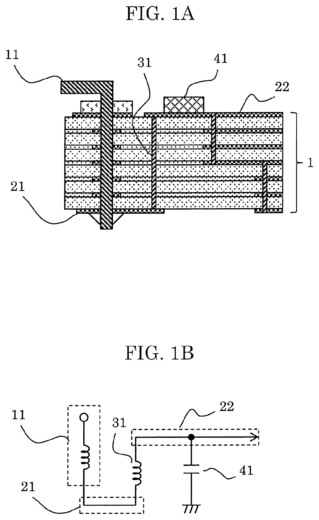
[0037]FIG. 1A is a cross-sectional view showing a configuration example of the multilayer circuit board input filter according to Embodiment 1. FIG. 1B is a diagram showing an equivalent circuit for describing electrical properties of the input filter in FIG. 1A.

[0038]The input filter in FIG. 1A is a filter circuit formed on multilayer circuit board 1, and includes input terminal 11, first wiring conductor 21, first via 31, second wiring conductor 22, and first input capacitor 41. This input filter, for example, (i) is a low-pass filter (LPF) that inputs a power-supply voltage supplied by multilayer circuit board 1 and reduces noise included in the power-supply voltage, and (ii) supplies the noise-reduced power-supply voltage to another circuit in multilayer circuit board 1.

[0039]Multilayer circuit board 1 (i) has a configuration in which insulating s...

embodiment 2

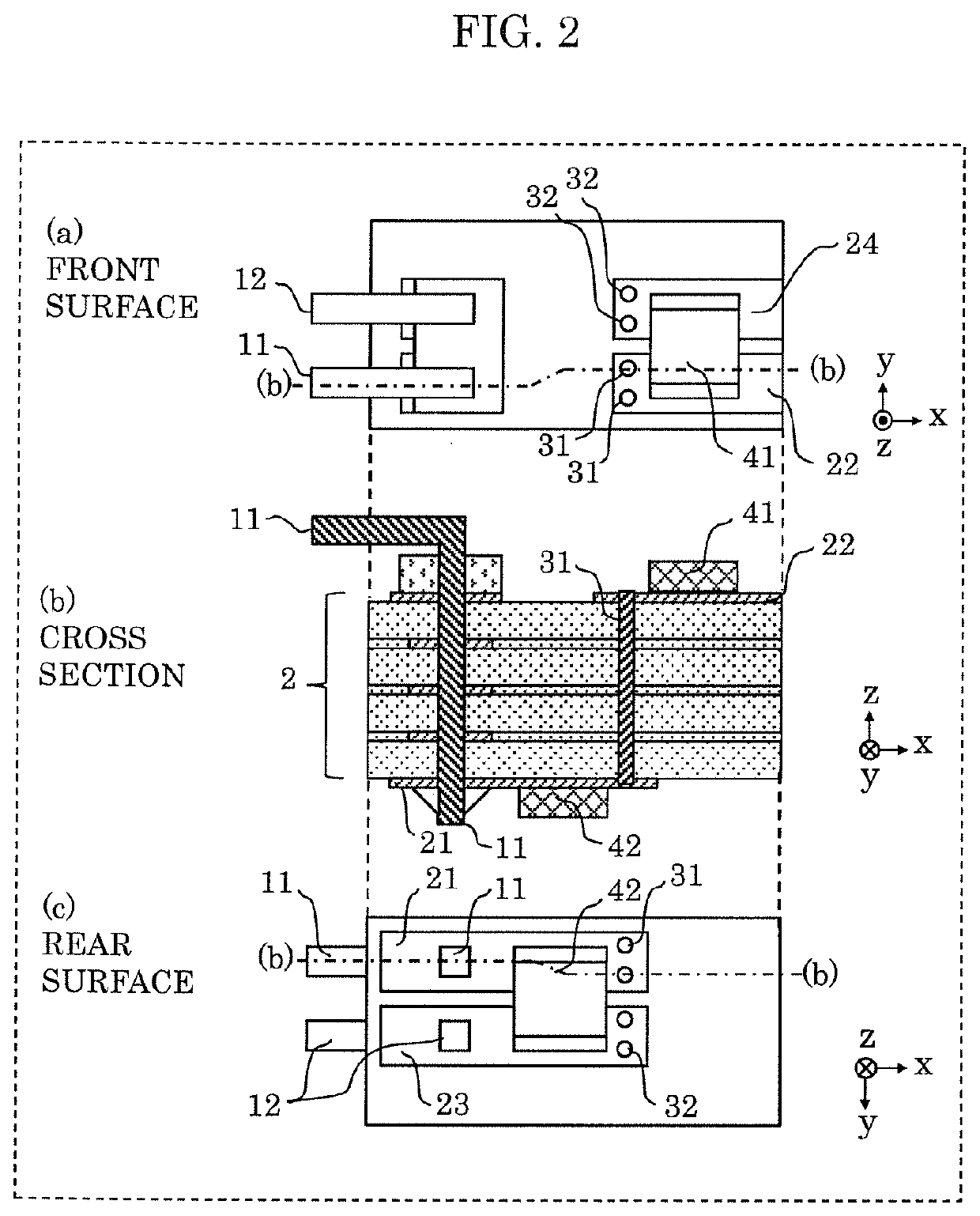
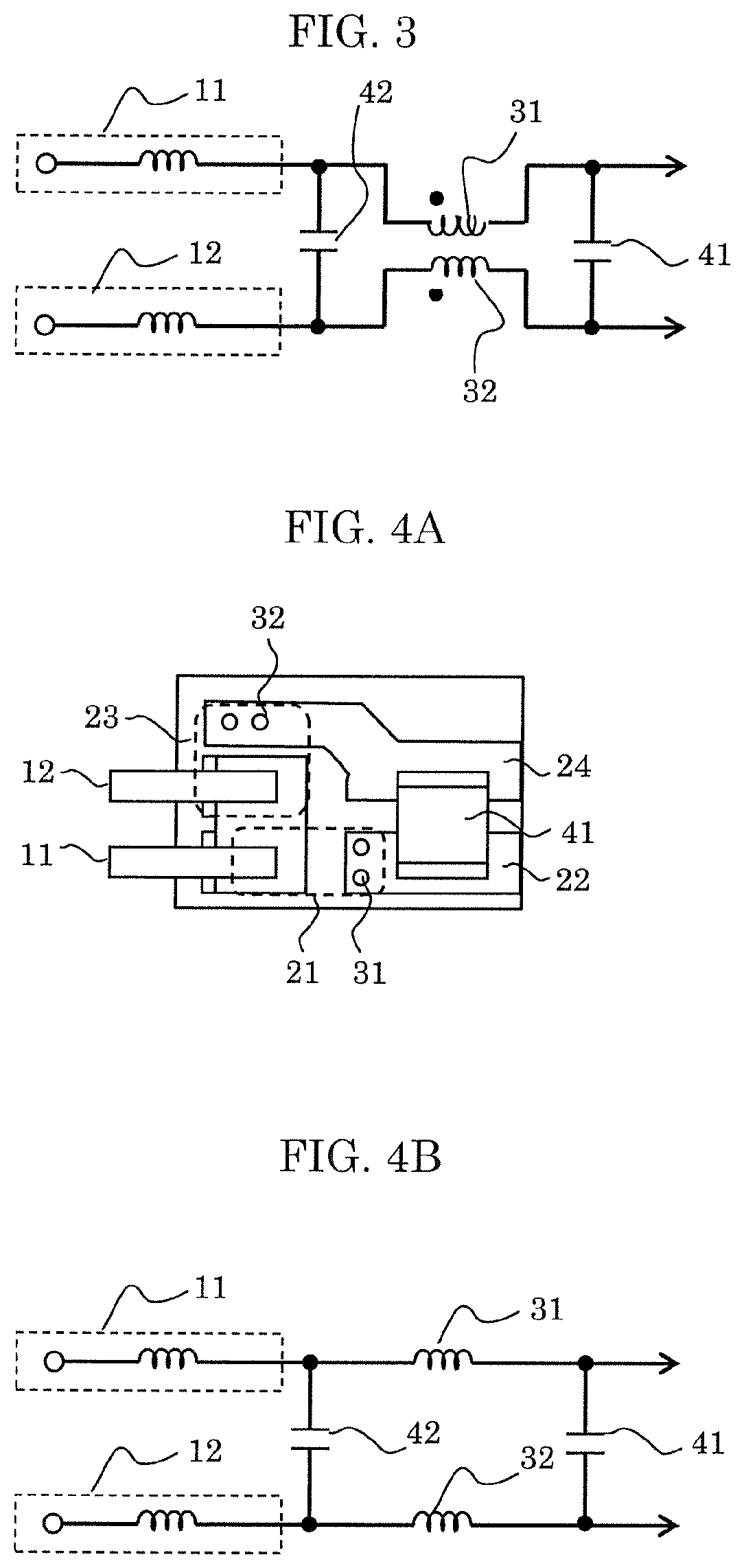
[0053]FIG. 2 is a diagram showing (a) front surface, (b) cross section, and (c) rear surface of a multilayer circuit board input filter according to Embodiment 2. (b) in the drawing is a cross section along dash-dotted line (b)-(b) shown in (a) front surface and (c) rear surface. FIG. 3 is a diagram showing an equivalent circuit for describing electrical properties of the input filter. The multilayer circuit board input filter in Embodiment 1 shown in FIG. 1 has a configuration in which one input line is applied thereto, but Embodiment 2 relates to a pair of two input lines, a power-supply line and a ground line. In FIG. 2, the power-supply line is the same as in the multilayer circuit board input filter according to Embodiment 1 shown in FIG. 1 and is therefore given the same reference numeral.

[0054]Note that the multilayer circuit board in Embodiment 2 is named multilayer circuit board 2 to distinguish between the multilayer circuit board in FIG. 1. Second input capacitor 42 is co...

embodiment 3

[0068]In the multilayer circuit board input filter in FIG. 2 described in the above Embodiment 2, second input capacitor 42 including the n filter can be omitted or have its electrostatic capacitance reduced due to the configuration described in Embodiment 3.

[0069]FIG. 5 is a diagram showing (a) even-numbered inner layer, (b) odd-numbered inner layer, (c) cross section, and (d) cross section in a configuration example of a multilayer circuit board input filter according to Embodiment 3. In FIG. 5, the multilayer circuit board input filter is the same as the multilayer circuit board input filter according to Embodiment 2 shown in FIG. 2, and is therefore given the same reference numeral. A multilayer circuit board according to Embodiment 3 is named multilayer circuit board 3 to distinguish between the multilayer circuit board in FIG. 2. Multilayer circuit board 3 includes at least two wiring layers. The at least two wiring layers include at least one first inner layer and at least on...


PUM


Abstract

An advantageous effect of a low-pass filter that reduces high-frequency noise can be obtained by including an input terminal that extends from a front surface to a rear surface of a multilayer circuit board including a double-sided circuit board; a first wiring conductor having an end connected to the input terminal on the rear surface of the multilayer circuit board; a first via that extends from an other end of the first wiring conductor to the front surface of the multilayer circuit board; a second wiring conductor having an end connected to the first via on the front surface of the multilayer circuit board; and a first input capacitor disposed on the second wiring conductor; by being conductive due to the input terminal and the first via being configured in series; and including the first input capacitor.

Description

CROSS REFERENCE TO RELATED APPLICATIONS[0001]This application is a U.S. continuation application of PCT International Patent Application Number PCT / JP2018 / 004506 filed on Feb. 09, 2018, claiming the benefit of priority of U.S. Provisional Patent Application Number 62 / 457,515 filed on Feb. 10, 2017, the entire contents of which are hereby incorporated by reference.BACKGROUND1. Technical Field[0002]The present disclosure relates to a filter that is disposed on a multilayer circuit board on which an electronic circuit is mounted, and in particular to a multilayer circuit board filter that reduces high-frequency noise from a power-supply line, ground line, and the like.2. Description of the Related Art[0003]In recent years, multilayer circuit boards that are stacked insulating substrates on which wiring conductors such as copper foil are applied by printing, etc. have been used for making electronic equipment smaller. In multilayer circuit boards, electronic circuits are generally forme...

Claims


Application Information

Patent Timeline
Patent Type & Authority Applications(United States)
IPC IPC(8): H05K1/02H05K1/18H03H7/01
CPCH03H7/0115H05K1/181H05K1/0233H03H7/09H03H2001/0085H03H1/00H03H7/427
Inventor MINAMI, YOSHIHISAISHII, TAKUYA
Owner PANASONIC INTELLECTUAL PROPERTY MANAGEMENT CO LTD
Why Eureka
Try Eureka