Wafer handling chamber with moisture reduction

a technology of moisture reduction and handling chamber, which is applied in the direction of semiconductor/solid-state device manufacturing, basic electric elements, electric apparatus, etc., can solve the problems of delay in waiting for the next wafer to be brought back to equilibrium, oxidation of the wafer, and undesirable oxidation for forming unwanted products on the wafer

Active Publication Date: 2019-12-05
ASM IP HLDG BV
View PDF0 Cites 234 Cited by
  • Summary
  • Abstract
  • Description
  • Claims
  • Application Information

AI Technical Summary

Benefits of technology

[0006]For purposes of summarizing aspects of the invention and the advantages achieved over the related art, certain objects and advantages of the invention are described in this disclosure. Of course, it is to be understood that not necessarily all such objects or advantages may be achieved in accordance with any particu...

Problems solved by technology

In this process, moisture may accumulate on the wafer, resulting in oxidation of the wafer.
Oxidation is undesirable for forming unwanted products on the wafer.
Adjusting the pressure of the chamber may require changing the ambient conditions, which may cause a delay in waiting for a next wafer to be brought back to equilibrium.
In addition, an ability to reduce the pressure in the chamber is limited by pumping capacity.
Furthermore, increasing the flow of purging nitrogen gas is limited ...

Method used


Image

  • Wafer handling chamber with moisture reduction
  • Wafer handling chamber with moisture reduction

Examples


Embodiment Construction

[0018]Although certain embodiments and examples are disclosed below, it will be understood by those in the art that the invention extends beyond the specifically disclosed embodiments and / or uses of the invention and obvious modifications and equivalents thereof. Thus, it is intended that the scope of the invention disclosed should not be limited by the particular disclosed embodiments described below.

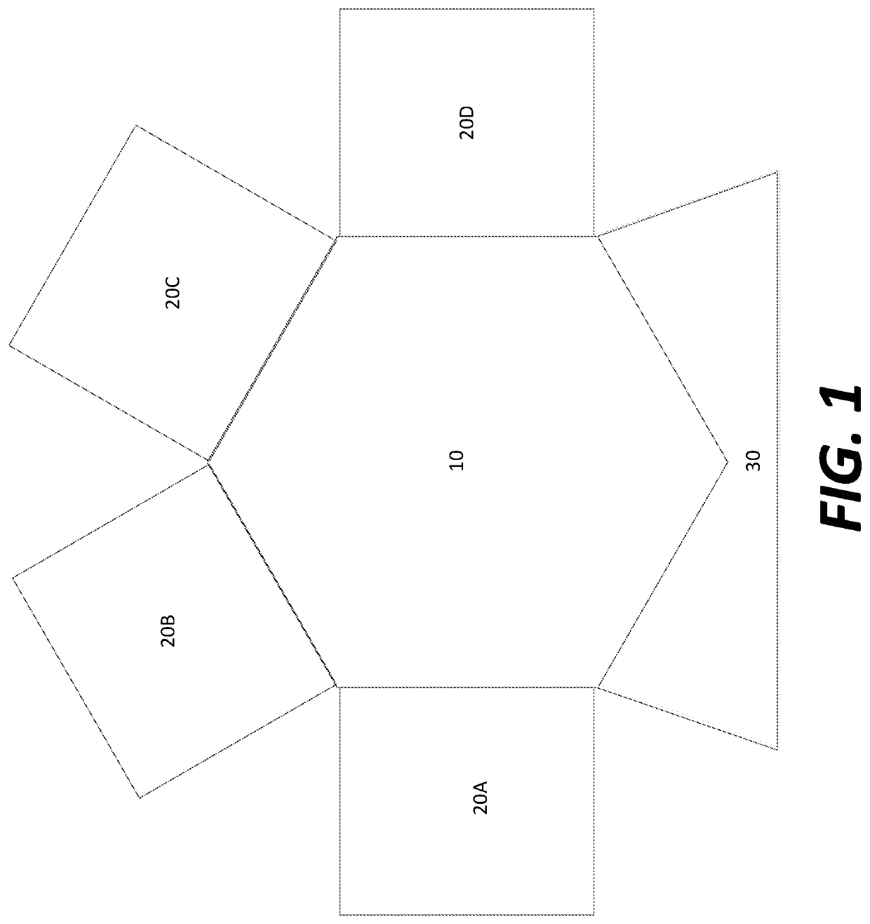
[0019]A semiconductor wafer processing system may comprise a number of different chambers. FIG. 1 illustrates a representative semiconductor wafer processing system. The system may comprise a wafer handling chamber 10, a number of reaction chambers 20A-20D, and a loadlock chamber 30. A semiconductor wafer may first enter the system from a cassette of wafers into the loadlock chamber 30. A gate valve disposed between the loadlock chamber 30 and the wafer handling chamber 10 may be lowered so that the semiconductor wafer may enter into the wafer handling chamber 10. Additional gate valve...


PUM


Abstract

An apparatus and method for reducing moisture within a wafer handling chamber is disclosed. The moisture reduction results in reduced oxidation of a wafer. The moisture reduction is made possible through use of valves and purging gas. Operation of the valves may result in improved localized purging.

Description

CROSS-REFERENCE TO RELATED APPLICATIONS[0001]This application is a Non-Provisional of, and claims priority to and the benefit of, U.S. Ser. No. 62 / 680,465 filed Jun. 4, 2018 and entitled “WAFER HANDLING CHAMBER WITH MOISTURE REDUCTION,” which is hereby incorporated by reference in its entirety for all purposes.FIELD OF THE INVENTION[0002]The present disclosure generally relates to semiconductor processing tools. More particularly, the disclosure relates to a wafer handling mechanism with a purge capability to reduce moisture around a wafer.BACKGROUND OF THE DISCLOSURE[0003]Wafers can travel through several different chambers during processing. For example, a wafer may go from a cassette in which the wafer is stored, into a wafer handling chamber. The wafer may go from the wafer handling chamber into a reaction chamber. In this process, moisture may accumulate on the wafer, resulting in oxidation of the wafer. Oxidation is undesirable for forming unwanted products on the wafer. In ad...

Claims


Application Information

Patent Timeline
IPC IPC(8): H01L21/673H01L21/67
CPCH01L21/67201H01L21/67393H01L21/67017H01L21/67126H01L21/67196H01L21/67207H01L21/67772H01L21/67742H01L21/68707H01L21/67253H01L21/67276H01L21/302
Inventor RAISANEN, PETRIJOHNSON, WARD
Owner ASM IP HLDG BV
Why Eureka
Try Eureka