Semiconductor memory device

Active Publication Date: 2020-01-16
SK HYNIX INC
View PDF7 Cites 3 Cited by
  • Summary
  • Abstract
  • Description
  • Claims
  • Application Information

AI Technical Summary

Benefits of technology

This patent is about a type of semiconductor memory that can hold a lot of data and has good electrical properties.

Problems solved by technology

In recent years, there has been a demand for large capacity and high integration of a semiconductor memory device in step with multifunctionality of an information communication device, and the structures of a logic circuit and wiring lines included in the semiconductor memory device for the operation and electrical coupling of the semiconductor memory device have been complicated.

Method used


Image

  • Semiconductor memory device
  • Semiconductor memory device
  • Semiconductor memory device

Examples


Embodiment Construction

[0019]Hereinafter, a semiconductor memory device will be described below with reference to the accompanying drawings through various embodiments.

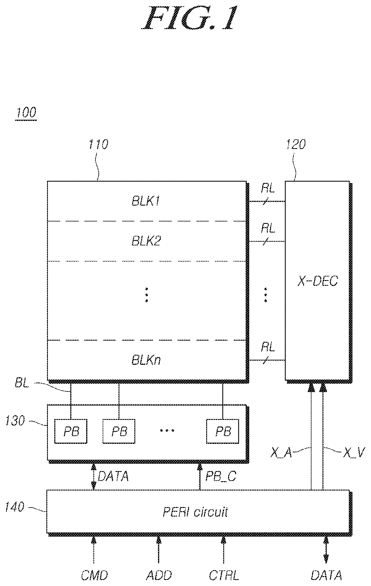
[0020]FIG. 1 is a block diagram illustrating an exemplary configuration of a semiconductor memory device in accordance with an embodiment of the present disclosure.

[0021]Referring to FIG. 1, a semiconductor memory device 100, in accordance with an embodiment, may include a memory cell array 110, a row decoder 120, a page buffer circuit 130 and a peripheral circuit 140.

[0022]The memory cell array 110 may include a plurality of memory blocks BLK1 to BLKn. While not shown, each of the memory blocks BLK1 to BLKn may include a plurality of memory cells. A memory cell may be accessed by a word line and a bit line. A memory cell may be a volatile memory cell which loses data stored therein in the case where power supply is interrupted, or may be a nonvolatile memory cell which retains data stored therein even though power supply is interrupted.

[00...


PUM


Abstract

A semiconductor memory device includes a substrate including a cell region and a slimming region; a logic structure disposed over the substrate, the logic structure including logic circuit elements and bottom wiring lines electrically coupled to the logic circuit elements; a source plate disposed over the logic structure; a memory structure including a plurality of memory cells and a plurality of gate electrode layers, wherein the plurality of memory cells are disposed over the source plate of the cell region and a plurality of gate electrode layers are stacked over the source plate of the cell region and the slimming region to be separated from one another and are coupled to the plurality of memory cells; and a first slit cutting the source plate at a boundary between the cell region and the slimming region, wherein the source plate of the slimming region is floated regardless an operation of the memory cells and the logic circuit elements.

Description

CROSS-REFERENCE TO RELATED APPLICATION[0001]The present application claims priority under 35 U.S.C. 119(a) to Korean Patent Application No. 10-2018-0081062 on Jul. 12, 2018, which is incorporated herein by reference in its entirety.BACKGROUND1. Technical Field[0002]Various embodiments generally relate to a semiconductor memory device and, more particularly, to a semiconductor memory device of a three-dimensional structure.2. Related Art[0003]In recent years, there has been a demand for large capacity and high integration of a semiconductor memory device in step with multifunctionality of an information communication device, and the structures of a logic circuit and wiring lines included in the semiconductor memory device for the operation and electrical coupling of the semiconductor memory device have been complicated. Accordingly, a semiconductor memory device having excellent electrical characteristics is required.SUMMARY[0004]A large capacity, high integration semiconductor memor...

Claims


Application Information

Patent Timeline
IPC IPC(8): H01L27/11582H01L27/11573H01L27/11565H01L27/11575
CPCH01L27/11565H01L27/11573H01L27/11582H01L27/11575G11C5/06H10B43/10H10B43/50H10B43/27H10B41/35H10B41/41H10B41/27H10B43/40
Inventor KIM, JIN-HOKIM, YOUNG-KIKIM, JEONG-HWANSUNG, SANG-HYUN
Owner SK HYNIX INC
Why Eureka
Try Eureka