Solid-state imaging device and electronic device

a technology of solid-state imaging and electronic devices, which is applied in the direction of color television details, television system details, television systems, etc., can solve the problems of high conversion efficiency of charge-voltage conversion units and large voltage amplitude after conversion, so as to improve the transfer efficiency of charge from charge storage units to charge-voltage conversion units via the transfer unit

Active Publication Date: 2020-02-13
SONY SEMICON SOLUTIONS CORP
View PDF0 Cites 8 Cited by
  • Summary
  • Abstract
  • Description
  • Claims
  • Application Information

AI Technical Summary

Benefits of technology

[0015]According to the first to third aspects of the present technology, the transfer efficiency of the charge from the charge storage unit to the charge-voltage conversion unit via the transfer unit can be improved.
[0016]Note that effects described here are not necessarily limited, and any of effects described in the present disclosure may be exhibited.

Problems solved by technology

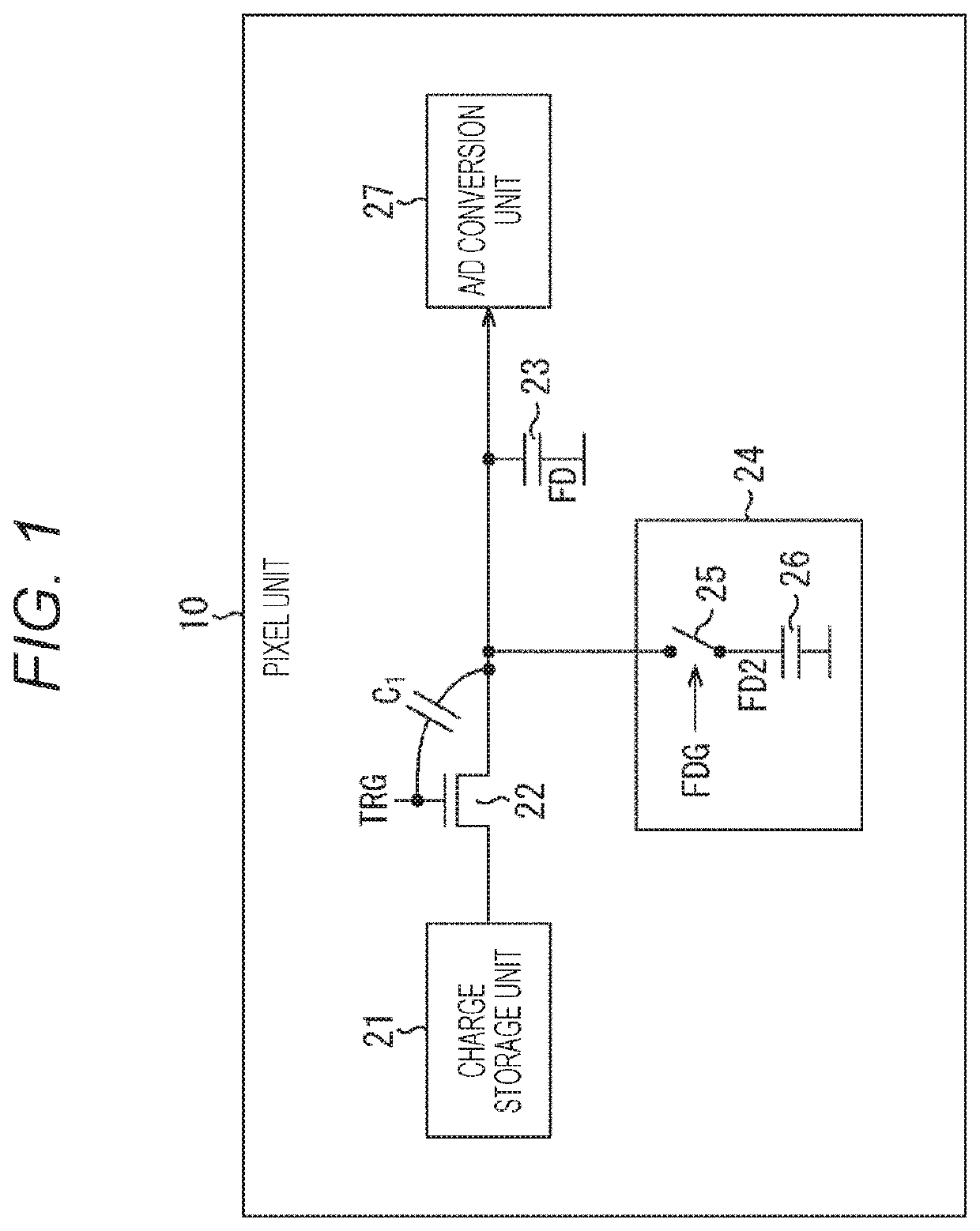
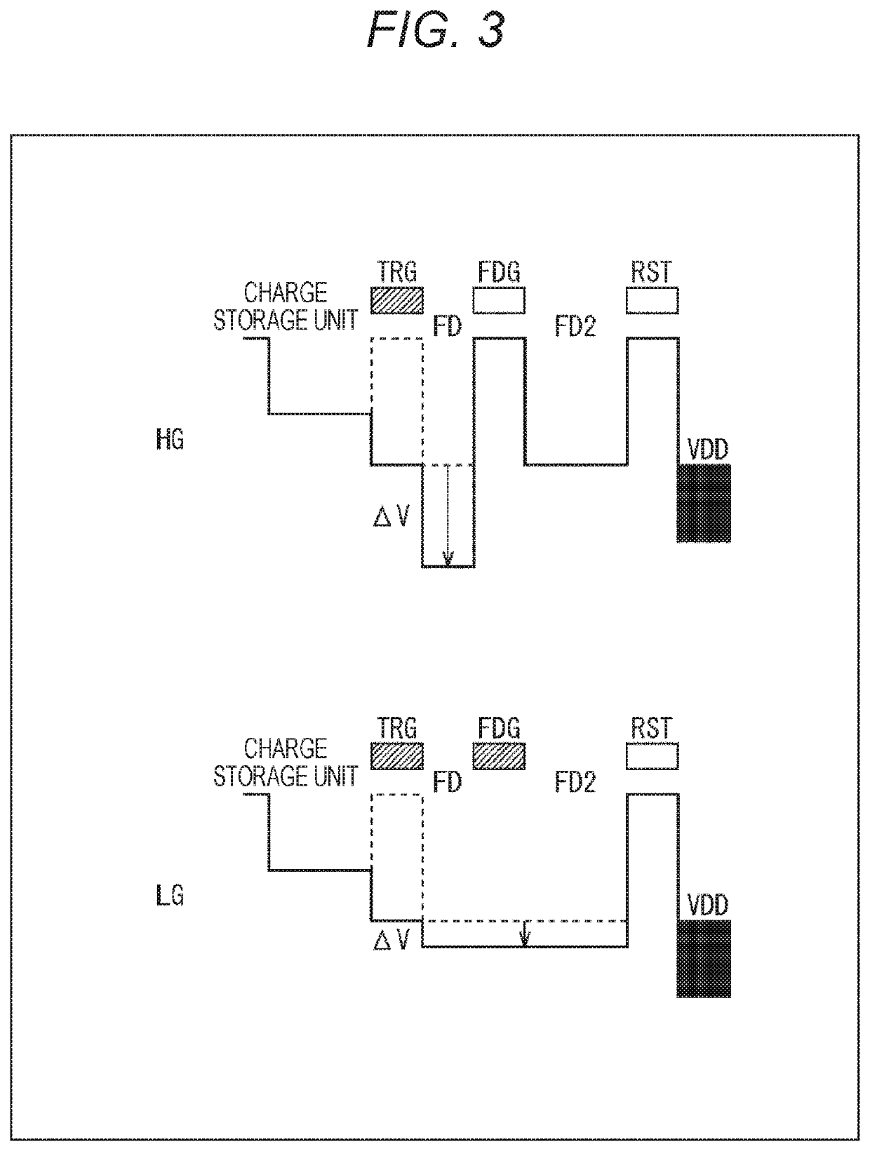
Meanwhile, in the case of disconnecting the additional capacitance from the FD, the conversion efficiency of the charge-voltage conversion unit becomes high and voltage amplitude after conversion becomes large even with a small charge amount.

Method used


Image

  • Solid-state imaging device and electronic device
  • Solid-state imaging device and electronic device
  • Solid-state imaging device and electronic device

Examples


application example

to Moving Bodies

[0246]The technology according to the present disclosure (present technology) can be applied to various products. For example, the technology according to the present disclosure may be realized as a device mounted on any type of moving bodies including an automobile, an electric automobile, a hybrid electric automobile, a motorcycle, a bicycle, a personal mobility, an airplane, a drone, a ship, a robot, and the like.

[0247]FIG. 39 is a block diagram illustrating a schematic configuration example of a vehicle control system as an example of a moving body control system to which the technology according to the present disclosure is applicable.

[0248]A vehicle control system 12000 includes a plurality of electronic control units connected through a communication network 12001. In the example illustrated in FIG. 39, the vehicle control system 12000 includes a drive system control unit 12010, a body system control unit 12020, a vehicle exterior information detection unit 12...


PUM

PropertyMeasurementUnit
voltageaaaaaaaaaa
chargeaaaaaaaaaa
capacitanceaaaaaaaaaa

Abstract

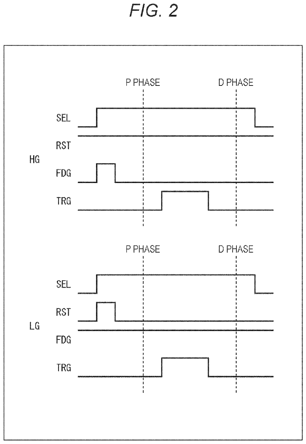
A solid-state imaging device and electronic device with improved charge transfer efficiency from a charge storage unit to a charge-voltage conversion unit via a transfer gate are disclosed. In one example, the solid-state imaging device is configured so that, before an A/D conversion operation for signal level acquisition, a switching unit switches a state to the LG state at least once and to the HG state at least once. A transfer unit is configured to transfer the charge stored in the charge storage unit to the charge-voltage conversion unit at least twice when the state is being switched to the LG state and when the state is being switched to the HG state. A charge-voltage conversion unit adds the charge that is transferred for the LG state and the HG state and convert the added charge into a voltage signal.

Description

TECHNICAL FIELD[0001]The present technology relates to a solid-state imaging device and an electronic device, and in particular relates to a solid-state imaging device and an electronic device for enabling improvement of transfer efficiency of a charge from a charge storage unit to a charge-voltage conversion unit via a transfer gate.BACKGROUND ART[0002]Conventionally, in solid-state imaging devices represented by complementary metal-oxide semiconductor (CMOS) image sensors, a configuration to connect or disconnect an additional capacitance to or from a floating diffusion (FD) as a charge-voltage conversion unit is known as a method of improving low illuminance characteristics while securing a saturation signal amount of each pixel (for example, see Patent Document 1).[0003]In the case of connecting the additional capacitance to the FD, a charge amount storable in the charge-voltage conversion unit increases, and thus improvement of a dynamic range of a pixel value becomes possible....

Claims


Application Information

Patent Timeline
Patent Type & Authority Applications(United States)
IPC IPC(8): H04N5/3745
CPCH04N5/37455H04N25/59H04N25/778H04N25/77H04N25/75H04N25/772
Inventor TAKATSUKA, TAKAFUMISUGIMORI, YUSAKU
Owner SONY SEMICON SOLUTIONS CORP
Why Eureka
Try Eureka