
Semiconductor manufacturing component comprising deposition layer covering interlayer boundary and manufacturing method thereof

a manufacturing component and semiconductor technology, applied in the direction of superimposed coating process, plasma technique, coating, etc., can solve the problems of deteriorating a material characteristic of the final product, component itself being exposed to plasma and thus damaged, and affecting the uniformity of the energy distribution in such a case of the application of such rfs, so as to improve the durability of the product, reduce the production time, and facilitate etching

Active Publication Date: 2020-02-27
TOKAI CARBON CO LTD
View PDF3 Cites 0 Cited by
  • Summary
  • Abstract
  • Description
  • Claims
  • Application Information

AI Technical Summary

Benefits of technology

Example embodiments described herein describe a semiconductor manufacturing component and method that includes a deposition layer covering an interlayer boundary, which can prevent the growth of abnormal crystals and improve product durability. Additionally, a plasma-resistant layer can be formed when the semiconductor manufacturing component is exposed to plasma, which can further protect the interlayer boundary from etching. Controlling the flow rate and deposition speed of each layer can also reduce production time and improve efficiency of the product manufacturing process.

Problems solved by technology

However, the uniform energy distribution in such a case of the application of such RFs may not be achieved only by controlling an output of the RFs.
Herein, such a component itself may be exposed to plasma and thus damaged.
However, when forming a thick deposition layer at a time to deposit a plasma-resistant material in the semiconductor manufacturing component, various issues may occur therefrom.
Such abnormal crystal structure, which is initially generated in a small size, may continuously grow while such continuous deposition is being performed, and may thus affect all or some of semiconductor manufacturing components and result in deteriorating a material characteristic of a final product.

Method used


Image

  • Semiconductor manufacturing component comprising deposition layer covering interlayer boundary and manufacturing method thereof
  • Semiconductor manufacturing component comprising deposition layer covering interlayer boundary and manufacturing method thereof
  • Semiconductor manufacturing component comprising deposition layer covering interlayer boundary and manufacturing method thereof

Examples


Embodiment Construction

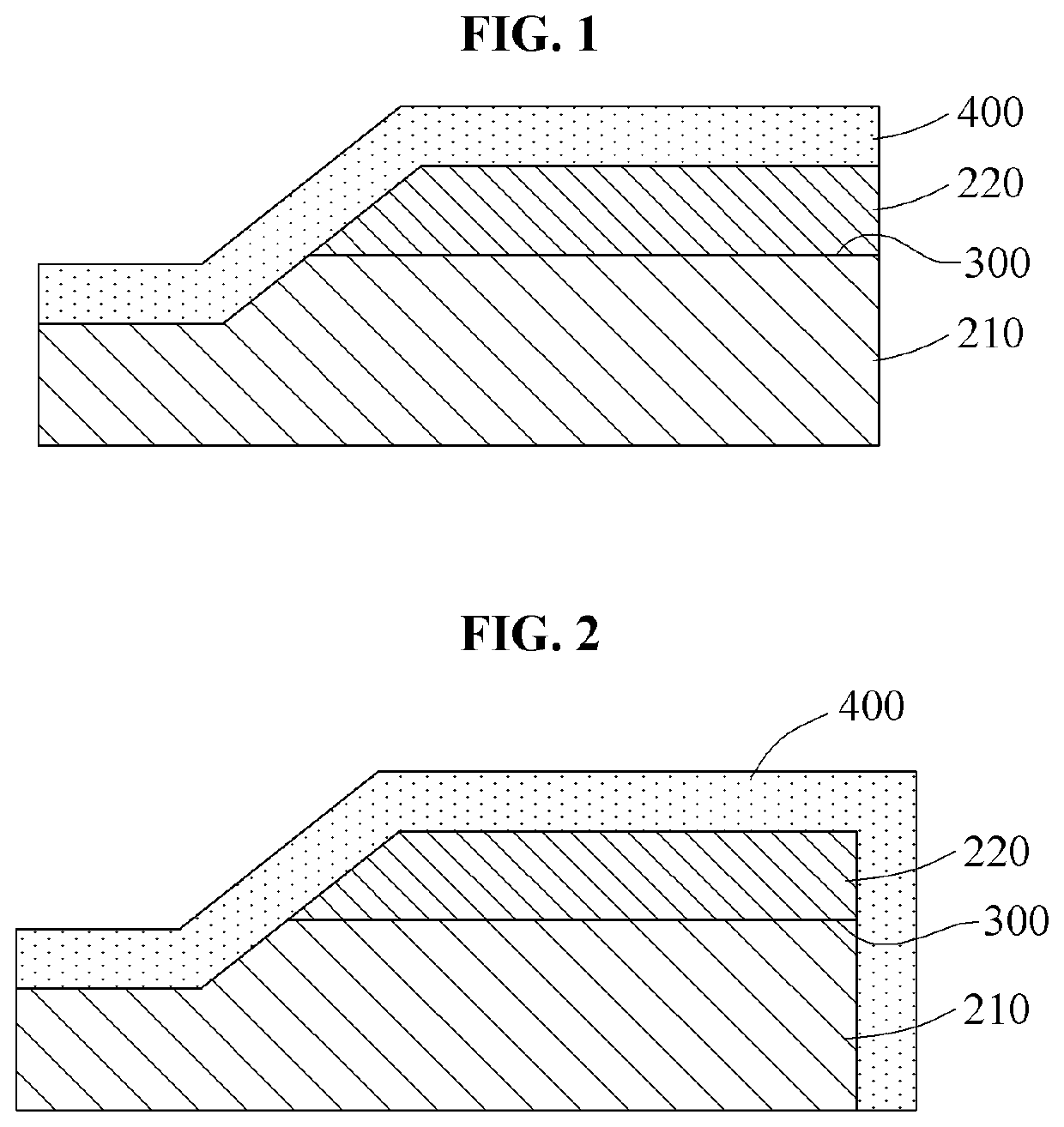
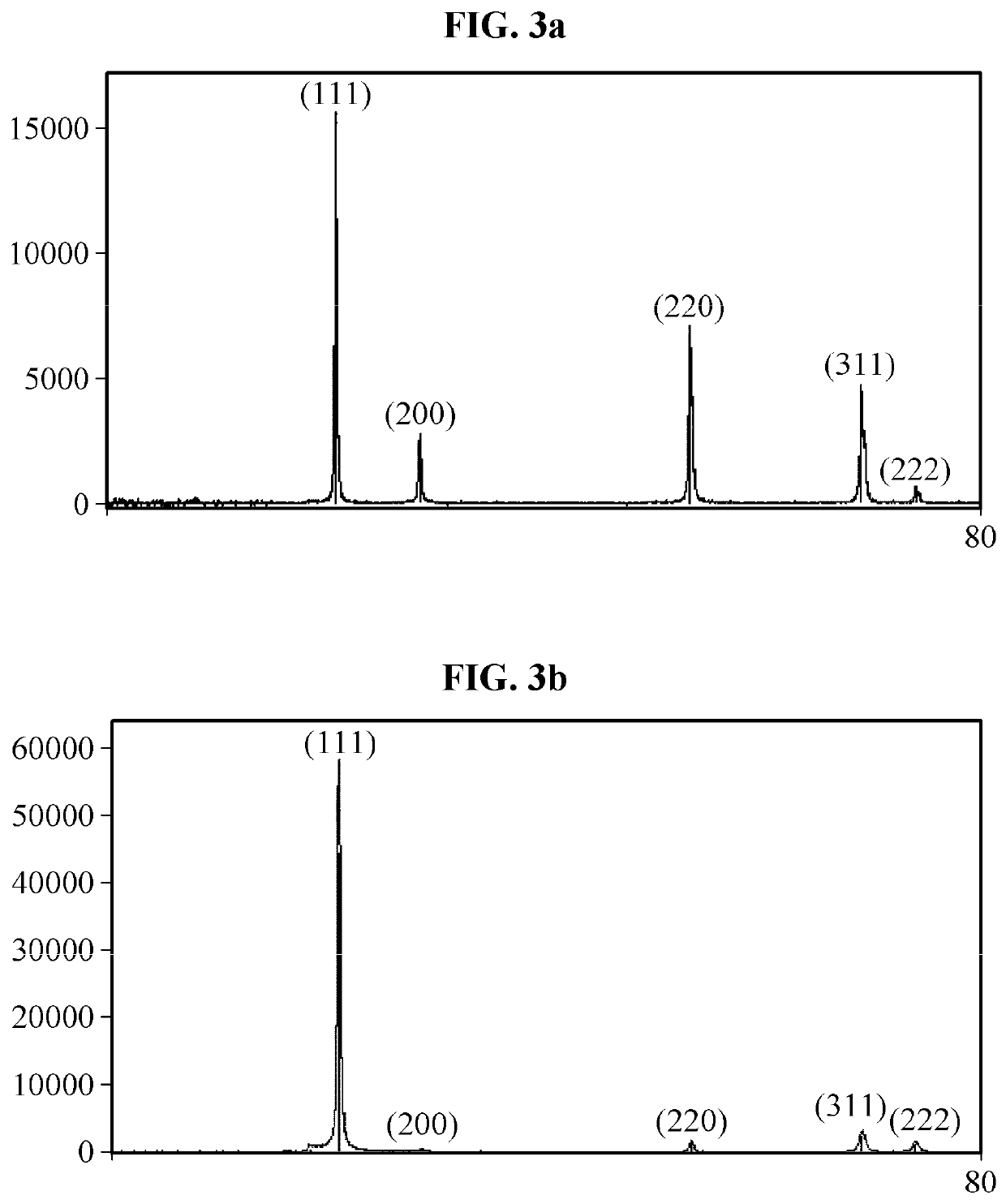
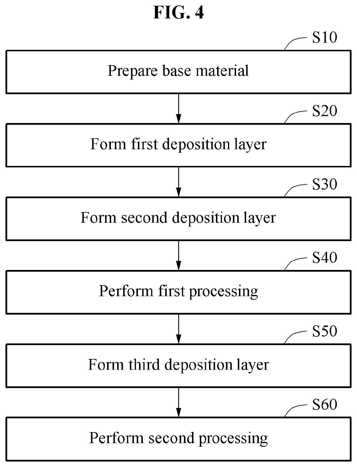
[0040]Hereinafter, example embodiments will be described with reference to the accompanying drawings, wherein like reference numerals refer to the like elements throughout.

[0041]However, various changes, modifications, and equivalents of the methods, apparatuses, and / or systems described herein will be apparent after an understanding of the disclosure of this application. The features described herein may be embodied in different forms, and are not to be construed as being limited to the examples described herein. Rather, the examples described herein have been provided merely to illustrate some of the many possible ways of implementing the methods, apparatuses, and / or systems described herein that will be apparent after an understanding of the disclosure of this application.

[0042]The terminology used herein is for the purpose of describing particular embodiments only and is not intended to be limiting the present disclosure. As used herein, the singular forms “a,”“an,” and “the,” a...


PUM

PropertyMeasurementUnit
thicknessaaaaaaaaaa
speedaaaaaaaaaa
thicknessaaaaaaaaaa

Abstract

The present invention relates to a semiconductor manufacturing component for manufacturing a semiconductor device by using a substrate such as a wafer in a dry etching process, and a manufacturing method thereof. The semiconductor manufacturing component comprising a deposition layer covering an interlayer boundary according to the present invention comprises: a base material containing carbon; a first deposition layer formed on the base material; a second deposition layer formed on the first deposition layer; and a third deposition layer formed on the first deposition layer and the second deposition layer, and formed to cover at least one portion of a boundary line between the first deposition layer and the second deposition layer.

Description

TECHNICAL FIELD[0001]Example embodiments relate to a semiconductor manufacturing component used to manufacture a semiconductor device using a substrate such as a wafer in a dry etching process and a method of manufacturing the same, and more particularly, to a semiconductor manufacturing component including a plurality of layers including a deposition layer covering an interlayer boundary and a method of manufacturing the same.BACKGROUND ART[0002]In general, a plasma processing method used in a semiconductor manufacturing process is one of dry etching processes through which a target is etched using gas.[0003]This method may include injecting etching gas into a reaction vessel and ionizing it, accelerating it to a wafer surface, and physically and chemically removing the wafer surface. The method is widely used because it is easy to control etching and is highly productive, and enables a formation of a fine pattern of tens of nanometers (nm).[0004]When performing plasma etching, par...

Claims


Application Information

Patent Timeline
Patent Type & Authority Applications(United States)
IPC IPC(8): C23C28/04H01L21/67C23C16/32C23C16/01
CPCC23C28/048C23C16/01H01L21/67069C23C16/325H01L21/3065H01L21/3213H05H1/46H01L21/02H01L21/68757H01L21/02274H01L21/32136H01L21/02315H01L21/0228H01L21/02041
Inventor LEE, SANG CHUL
Owner TOKAI CARBON CO LTD
Learn More