Display panel and display panel manufacturing method

Active Publication Date: 2020-03-12
WUHAN CHINA STAR OPTOELECTRONICS SEMICON DISPLAY TECH CO LTD
View PDF0 Cites 2 Cited by
  • Summary
  • Abstract
  • Description
  • Claims
  • Application Information

AI Technical Summary

Benefits of technology

The present invention describes a technology for protecting human eyes and improving the durability of OLED devices. It involves adding a layer of inorganic material that absorbs light in the UV wavelength band to the OLED layer. This layer prevents excessive light reflection and increases the stability and performance of the display.

Problems solved by technology

However, tendency of organic materials to be susceptible to water and oxygen erosion restricts the development of OLEDs.

Method used


Image

  • Display panel and display panel manufacturing method
  • Display panel and display panel manufacturing method
  • Display panel and display panel manufacturing method

Examples


Embodiment Construction

[0038]Each of the following embodiments is described with appending figures to illustrate specific embodiments of the present invention that are applicable. The terminologies of direction mentioned in the present invention, such as “upper”, “lower”, “front”, “rear”, “left”, “right”, “inner”, “outer”, “side surface” and etc., only refer to the directions of the appended figures. Therefore, the terminologies of direction are used for explanation and comprehension of the present invention, instead of limiting the present invention. In the figures, units with similar structures are marked with the same reference numerals.

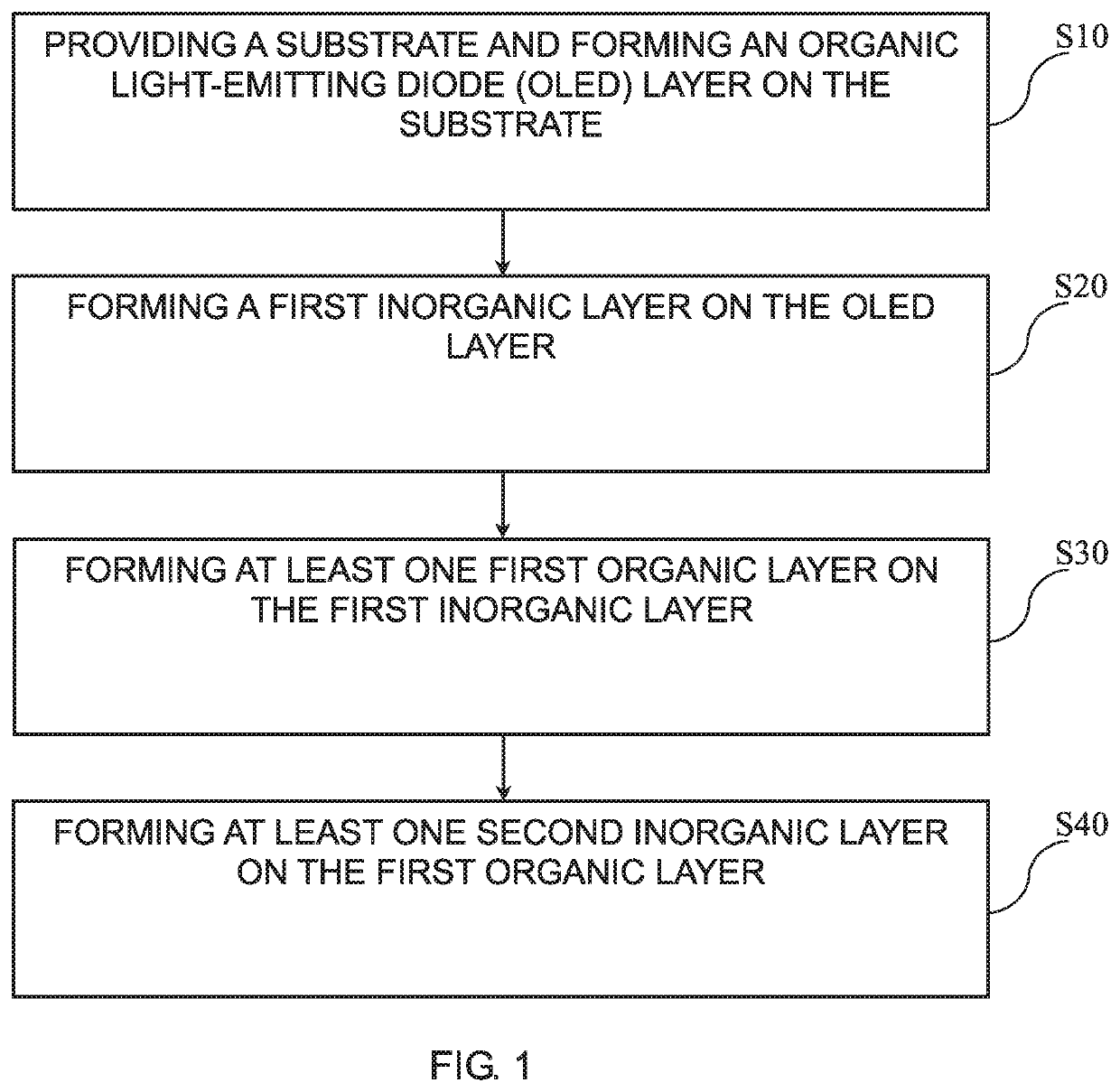
[0039]With reference to FIG. 1, FIG. 1 is a schematic flowchart of a display panel manufacturing method of the present invention. The method includes steps as follows.

[0040]Step S10 comprises providing a substrate and forming an organic light-emitting diode (OLED) layer on the substrate.

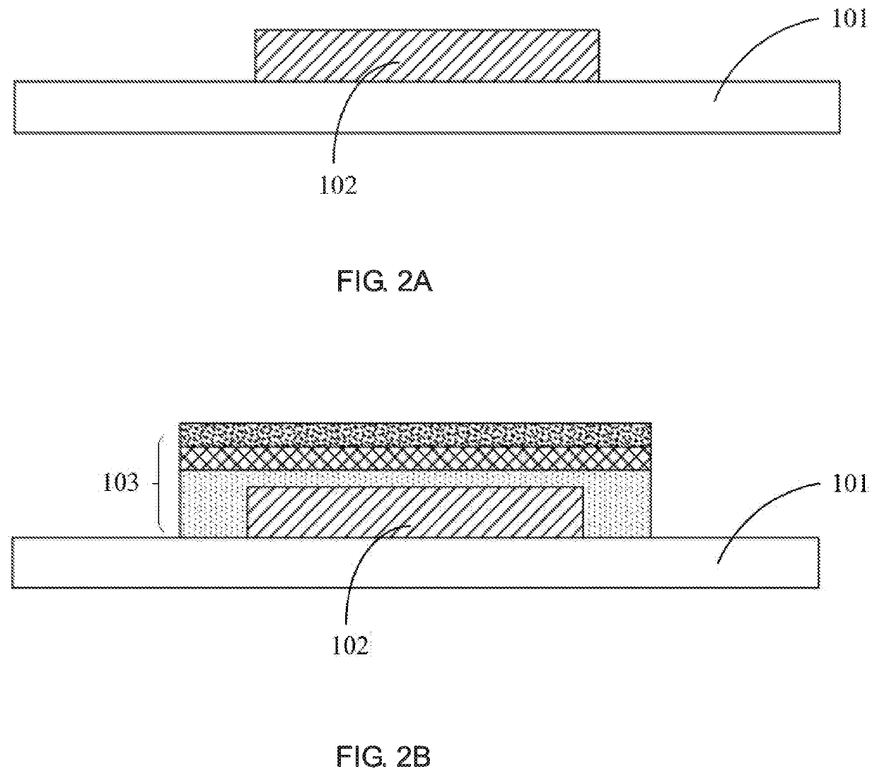
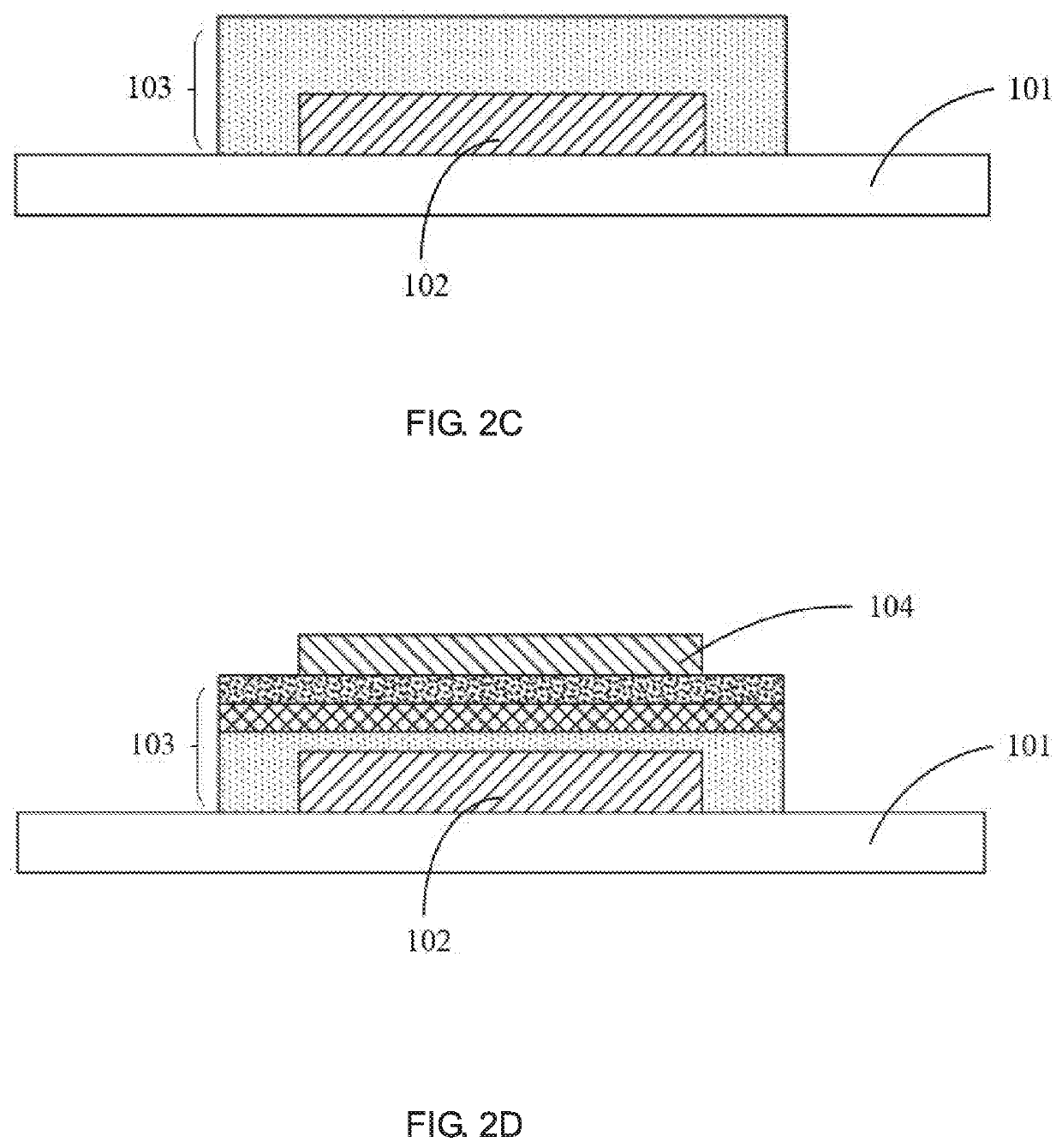
[0041]With reference to FIGS. 2A-2E, FIGS. 2A-2E are schematic views of the display ...


PUM


Abstract

A display panel and a display panel manufacturing method are provided. The display panel includes a thin film package layer; the thin film package layer includes at least one first inorganic layer, at least one first organic layer and at least one second inorganic layer. The first inorganic layer includes an inorganic material absorbing light of an ultraviolet wavelength band. Progressive decrease of a refractive index of the first inorganic layer prevents light emitted out of the OLEDs from sustaining total reflection in each contacting surface between layers and effectively increases stability and light performance of the display panel.

Description

FIELD OF INVENTION[0001]The present invention relates to display panel manufacturing fields, especially to a display panel and a display panel manufacturing method.BACKGROUND OF INVENTION[0002]In flexible display fields, organic light-emitting diodes (OLEDs) have an overwhelming advantage. However, tendency of organic materials to be susceptible to water and oxygen erosion restricts the development of OLEDs.[0003]Therefore, packaging OLED devices to be isolated from the external environment is critical to the stability of the OLED device. For flexible devices, the current popular packaging technology solution is encapsulating OLED devices through laminated organic / inorganic thin films.[0004]In the prior art, when light enters the organic buffer layer from the inorganic barrier layer or enters the air from the inorganic barrier layer, it is affected by the total reflection and luminous efficiency is therefore reduced.[0005]Therefore, there is a need for a display panel to solve the a...

Claims


Application Information

Patent Timeline
IPC IPC(8): H01L51/56H01L51/52
CPCH01L51/56H01L51/5275H10K50/8445H10K50/858H10K50/865H10K71/00H10K50/86
Inventor ZHANG, WENZHI
Owner WUHAN CHINA STAR OPTOELECTRONICS SEMICON DISPLAY TECH CO LTD
Why Eureka
Try Eureka