Differential trans-impedance amplifier

a technology of trans-impedance amplifier and differential amplifier, which is applied in differential amplifiers, amplifiers with semiconductor devices/discharge tubes, amplifier details, etc., can solve the problems of degraded gain and bandwidth performance, severe degraded performance, and photo diode biasing

Inactive Publication Date: 2020-03-19
NOKIA SOLUTIONS & NETWORKS OY
View PDF3 Cites 4 Cited by
  • Summary
  • Abstract
  • Description
  • Claims
  • Application Information

AI Technical Summary

Problems solved by technology

The large DC current saturates the receiver front-end, i.e. the TIA 2 and the MAs 3, and significantly degrades the gain and the bandwidth performances.
Such a large DC current is more than enough to saturate the receiver front-end and severely degrade performance.
Unfortunately, this technique suffers from two main drawbacks: 1) CC parasitic capacitance, and 2) photo diode biasing.
Furthermore, a large RC value impedes receiving high optical power levels as the DC current will be large and the voltage drop across the biasing resistor RC will be huge.
As a numerical example, an IDC of 10 μA leads to a 10 V drop on a 1 MΩ biasing resistor RC, which is not practical.
Moreover, the situation in coherent optical receivers is much worse as the photo diode DC current is around 1 mA and requires a biasing resistor RC of less than 1 kΩ for less than 1 V drop across the biasing resistor RC.

Method used


Image

  • Differential trans-impedance amplifier
  • Differential trans-impedance amplifier
  • Differential trans-impedance amplifier

Examples


Embodiment Construction

[0023]While the present teachings are described in conjunction with various embodiments and examples, it is not intended that the present teachings be limited to such embodiments. On the contrary, the present teachings encompass various alternatives and equivalents, as will be appreciated by those of skill in the art.

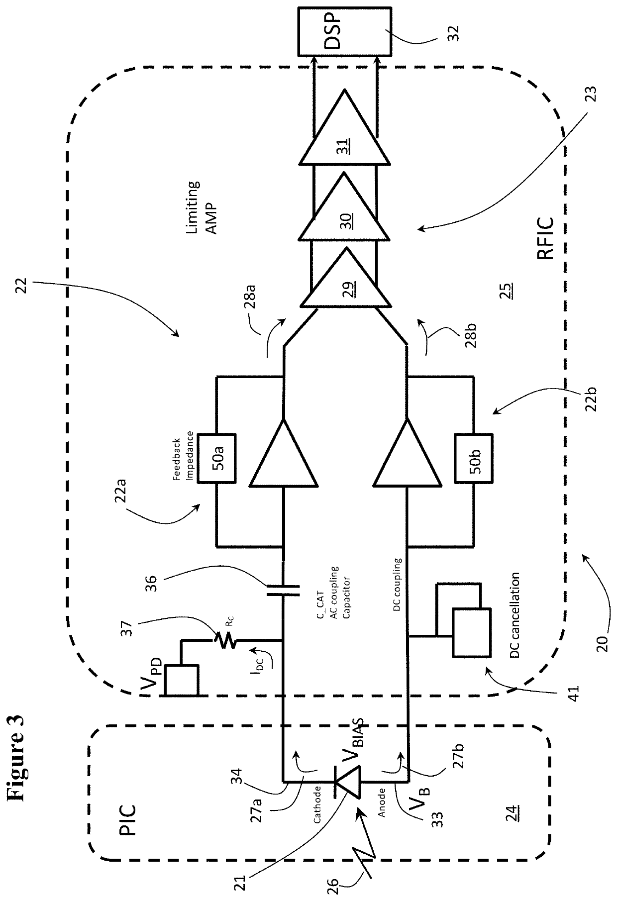
[0024]Compared to the above described single-ended schemes, a differential TIA scheme has advantages because the differential signal becomes 2× larger, while the RMS added random noise is only √2× larger, and therefore the differential TIA has increased SNR by only √2×. Moreover, differential TIA schemes provide better linearity for large input currents and low gain settings due to better common mode rejection ratio (CMRR) by 2nd harmonics rejection. Improved linearity is critical in PAM4 or higher order modulation schemes.

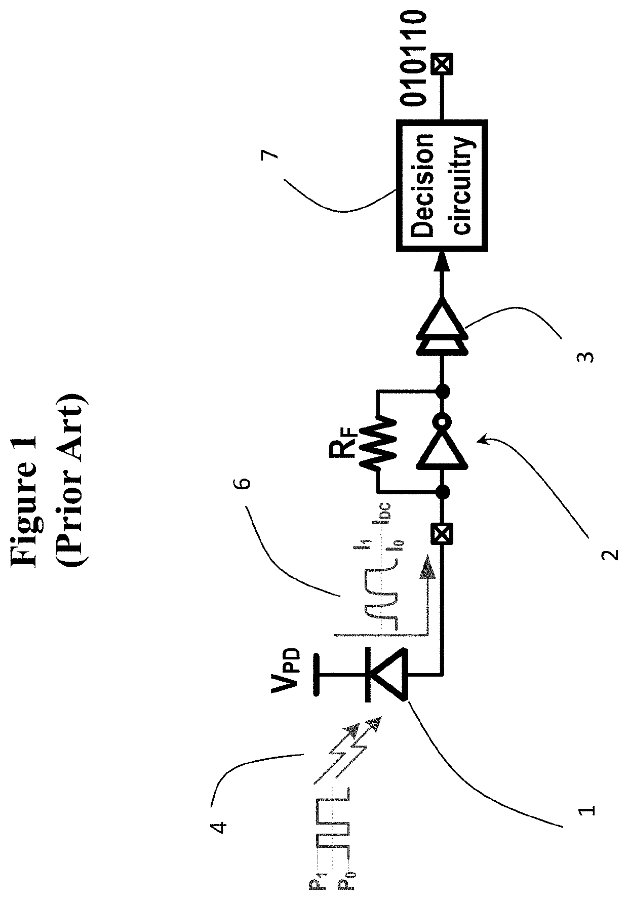
[0025]With reference to FIG. 3, an optical receiver 20, in accordance with the present invention, comprises of a photodetector, e.g. photo diode (PD)...


PUM


Abstract

In conventional high data rate receivers, the transmitted optical signal has poor extinction ratio and translates into a small modulated current with a large DC current, which saturates the receiver TIA and amplifiers, and significantly degrades the gain and bandwidth performance. Consequently, cancelling PD DC current in high data rate receivers is desired for proper operation. Differential TIA schemes, i.e. providing separate AC-coupled and DC-coupled paths, in parallel, provide better linearity for large input currents and low gain settings. To AC couple the PD to the TIA using passive AC-coupling circuitry, an AC-coupling capacitor (CC) is positioned between the PD and the TIA to block the DC current, while passing the modulated AC current to the TIA. A DC cancellation circuit may be provided, without a capacitor, to maintain the receiver input bias while suppressing any DC component generated by the PD for the DC-coupled path.

Description

CROSS REFERENCE TO RELATED APPLICATIONS[0001]This application is a continuation-in-part of and claims priority from U.S. patent application Ser. No. 16 / 135,914, entitled Optical Receivers with DC Cancellation and Offset Cancellation, filed Sep. 19, 2018, which is incorporated herein by reference.TECHNICAL FIELD[0002]The present invention relates to a trans-impedance amplifier (TIA) for a photodetector circuit, and in particular to a differential TIA with a mixed AC / DC coupling scheme.BACKGROUND[0003]A typical optical receiver front-end is composed of a photo diode (PD) 1 followed by a trans-impedance amplifier (TIA) 2 and main voltage amplifiers (MAs) 3 as shown in FIG. 1. The PD 1 receives a transmitted optical signal 4 and generates a PD output current 6 proportional to the received optical power of the transmitted optical signal 4. The ratio between PD output current 6 to the input optical power of the optical signal 4 is the photo diode responsivity (R). The TIA 2 converts the P...

Claims


Application Information

Patent Timeline
Patent Type & Authority Applications(United States)
IPC IPC(8): H03F3/45H03F3/183H03F3/10
CPCH03F3/10H03F3/45076H03F3/183H03F1/14H03F3/087H03F3/187H03F3/45475H03F3/45973
Inventor LIM, DAIHYUNRYLYAKOV, ALEXANDER
Owner NOKIA SOLUTIONS & NETWORKS OY
Why Eureka
Try Eureka