
Memory apparatus and method of controlling memory apparatus

Active Publication Date: 2020-03-26
SONY SEMICON SOLUTIONS CORP
View PDF0 Cites 1 Cited by
  • Summary
  • Abstract
  • Description
  • Claims
  • Application Information

AI Technical Summary

Benefits of technology

This patent is about a memory device and a method for controlling it that can prevent problems with the retention and rewriting lifetime of a specific memory cell. The device achieves this by keeping the voltage applied to a variable resistor within a certain range during data erasing. This helps to maintain the health of the memory cell and prevents it from becoming less effective over time.

Problems solved by technology

For example, in a case where the voltage applied to the memory cell is lower than an appropriate range, the retention characteristics are deteriorated.

Method used


Image

  • Memory apparatus and method of controlling memory apparatus
  • Memory apparatus and method of controlling memory apparatus
  • Memory apparatus and method of controlling memory apparatus

Examples


first embodiment

1. First Embodiment

[Configuration]

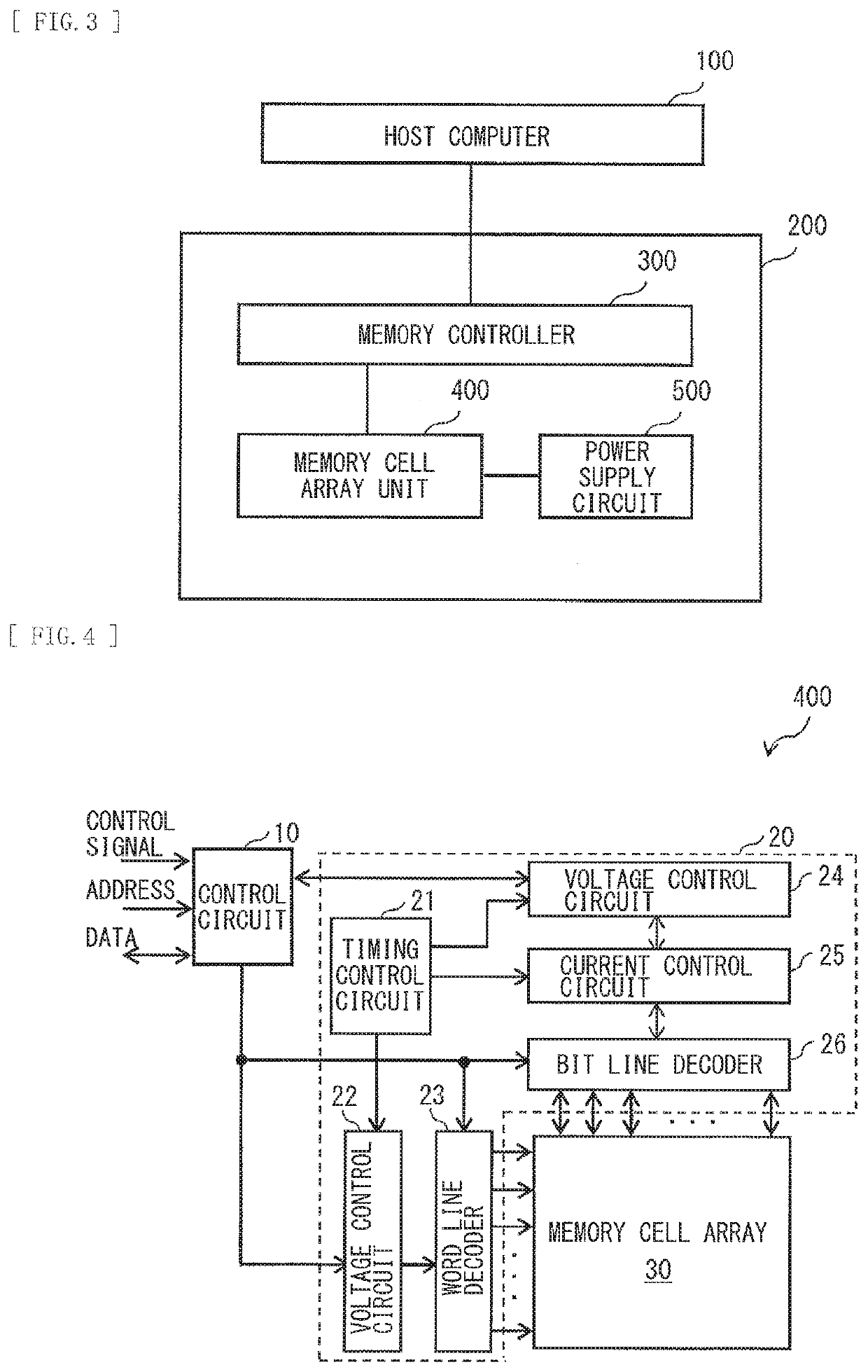
[0041]FIG. 3 illustrates an example of functional blocks of an information processing system according to a first embodiment of the disclosure. The information processing system includes a host computer 100 and a memory apparatus 200. The memory apparatus 200 includes a memory controller 300, one or a plurality of memory cell array units 400, and a power supply circuit 500. It is to be noted that FIG. 3 illustrates a state in which one memory cell array unit 400 is provided. The memory controller 300 corresponds to one specific example of a “determination unit” according to an embodiment of the disclosure.

[Host Computer 100]

[0042]The host computer 100 controls the memory apparatus 200. More specifically, the host computer 100 issues a command specifying a logical address of an access destination, and supplies the command and data to the memory apparatus 200. The host computer 100 also receives data outputted from the memory apparatus 200. Here, the ...

second embodiment

2. Second Embodiment

[0085]FIG. 13 illustrates an example of a reset operation in an information processing system according to a second embodiment of the disclosure. In the present embodiment, when erasing data, the drive circuit 20 applies an initial reset voltage Vrst1 to the memory cell MC to cause the selector SE to be in the selected state while the variable resistor VR is in the low resistance state, and then applies a late reset voltage Vrst3 lower than the initial reset voltage Vrst1 to the memory cell MC. The late reset voltage Vrst3 corresponds to one specific example of a “third voltage” according to an embodiment of the disclosure.

[0086]The current control circuit 25 sets the current limit value of the bit line BL to a current value (initial reset current Irst3) necessary for the variable resistor VR to be maintained in the low resistance state at a time point (t3 to be described later) when the selector SE changes from the non-selected state to the selected state, by ap...

modification example

3. Modification Example Common to Each Embodiment

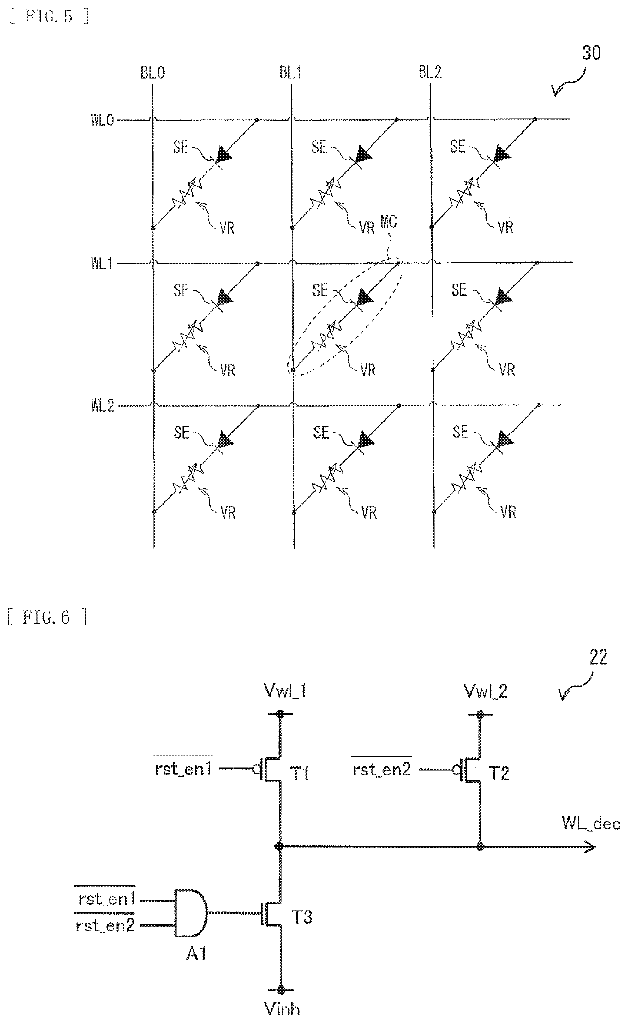
[0097]FIG. 16 illustrates a modification example of functional blocks of the memory cell array unit 400 included in the information processing system according to each of the above embodiments. A memory cell array unit 400 according to the present modification example corresponds to the memory cell array unit 400 according to each embodiment described above further including a current detection circuit 27.

[0098]The current detection circuit 27 detects a current flowing through the memory cell MC. The detection result (detection data) of the current detection circuit 27 is transmitted to the memory controller 300. As illustrated in FIG. 17, for example, the current detection circuit 27 includes inverters INV1 and INV2, a comparator CP1, NMOS transistors T1 and T2, and a current detection resistor R1.

[0099]A bit line BL coupled to the current detection resistor R1 is coupled to a non-inverting input terminal (+) of the comparator CP1. A...


PUM


Abstract

A memory apparatus includes a memory cell disposed at an intersection of a first wiring line and a second wiring line, and including a variable resistor and a selector, the variable resistor having a resistance state that changes to a first resistance state and a second resistance state, and a drive circuit that writes data to the memory cell by changing the variable resistor from the first resistance state to the second resistance state, and erases the data stored in the memory cell by changing the variable resistor from the second resistance state to the first resistance state. When erasing the data, the drive circuit changing in a stepwise manner a voltage applied to the memory cell, and changing in a stepwise manner a current limit value that limits a magnitude of a current flowing through the memory cell.

Description

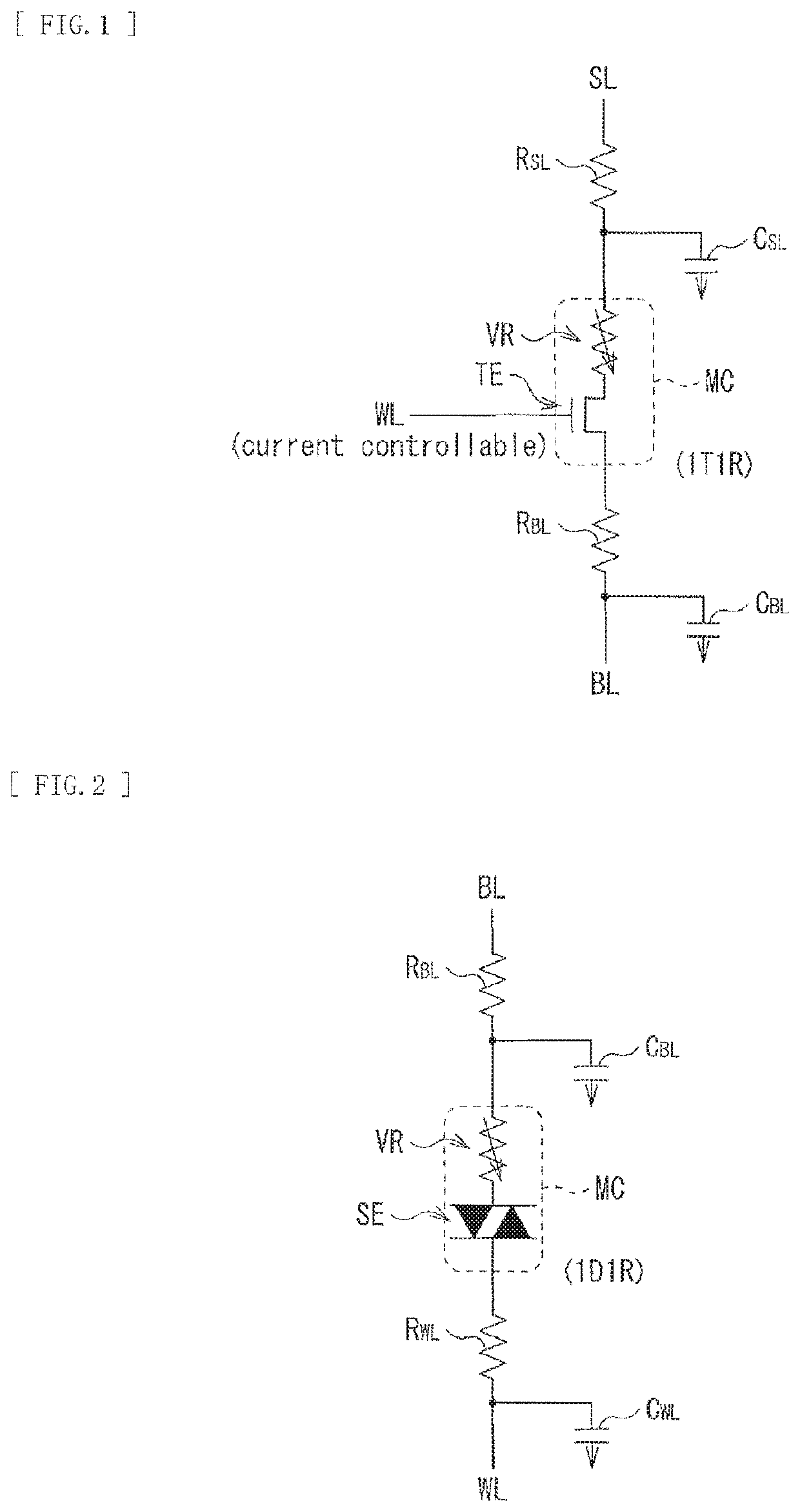
TECHNICAL FIELD[0001]The disclosure relates to a memory apparatus and a method of controlling the memory apparatus.BACKGROUND ART[0002]As a nonvolatile memory, there are known a resistive random access memory (ReRAM), a conduction bridge random access memory (CBRAM), a phase-change random access memory (PCRAM), a magnetoresistive random access memory (MRAM), a spin transfer torque random access memory (STTRAM), and the like. In ReRAM, a variable resistor that stores data according to a change in resistance is used as a nonvolatile memory element (see, for example, PTL 1 and PTL 2).[0003]As a configuration of a memory cell using the nonvolatile memory, a 1R (1 Resistor) type and a 1D1R (1 Diode 1 Resistor) type are known. A cross-point type memory apparatus is known in which such memory cells are disposed at intersections of a plurality of bit lines and a plurality of word lines.CITATION LISTPatent Literature[0004]PTL 1: Japanese Unexamined Patent Application Publication No. 2011-243...

Claims


Application Information

Patent Timeline
IPC IPC(8): G11C13/00
CPCG11C13/0069G11C2013/0045G11C13/004G11C13/0038G11C13/0097G11C13/003G11C2213/76G11C13/0026G11C13/0028G11C2013/0078G11C13/0061G11C13/0004
Inventor MORI, YOTAROKITAGAWA, MAKOTOOKUNO, JUNTERADA, HARUHIKO
Owner SONY SEMICON SOLUTIONS CORP
Learn More