Methods and apparatus to eliminate wafer bow for CVD and patterning hvm systems

a technology of cvd and patterning, applied in the direction of vacuum evaporation coating, basic electric elements, coatings, etc., can solve the problems of poor process uniformity, and achieve the effect of reducing or controlling the substrate bow or warpage and high density memory device fabrication

Active Publication Date: 2020-03-26
APPLIED MATERIALS INC
View PDF2 Cites 4 Cited by
  • Summary
  • Abstract
  • Description
  • Claims
  • Application Information

AI Technical Summary

Benefits of technology

[0007]The present disclosure generally provides a method and apparatus to minimize or control substrate bow or warpage in high density memory device fabrication.

Problems solved by technology

Such increased density introduces manufacturing process challenges such as bow or warpage of the underlying substrate.
Bow or warpage of the substrate creates challenges in handling of the substrate as well as depositing subsequent layers and / or depositing or patterning hardmask films.
Excessive substrate bow may also lead to arcing which may damage process kits, lead to poor process uniformity due to uncontrolled parasitic local discharges, variations in the gaps or spacing above or below the substrate, and / or substrate temperature variations.

Method used


Image

  • Methods and apparatus to eliminate wafer bow for CVD and patterning hvm systems
  • Methods and apparatus to eliminate wafer bow for CVD and patterning hvm systems
  • Methods and apparatus to eliminate wafer bow for CVD and patterning hvm systems

Examples


Embodiment Construction

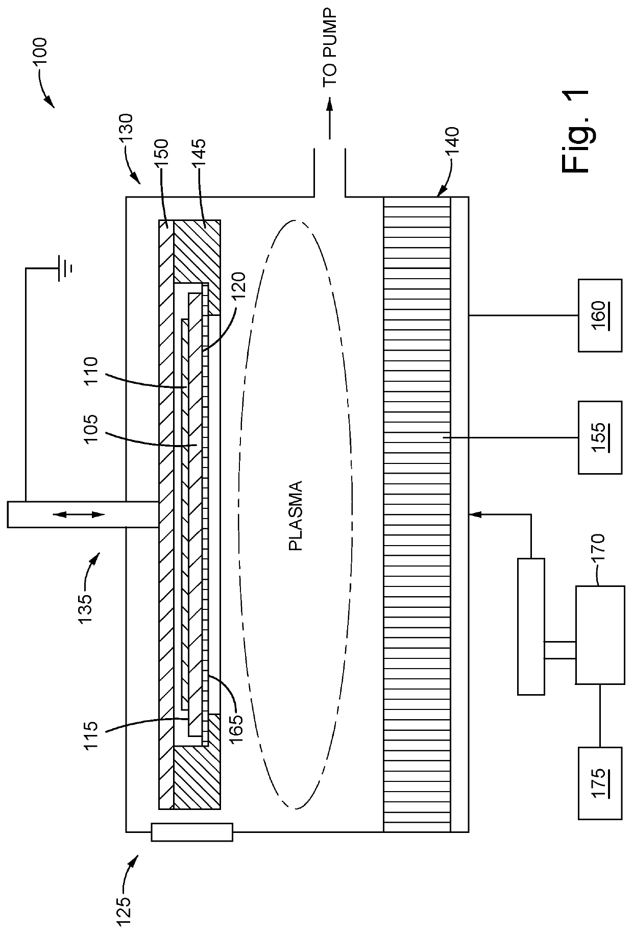
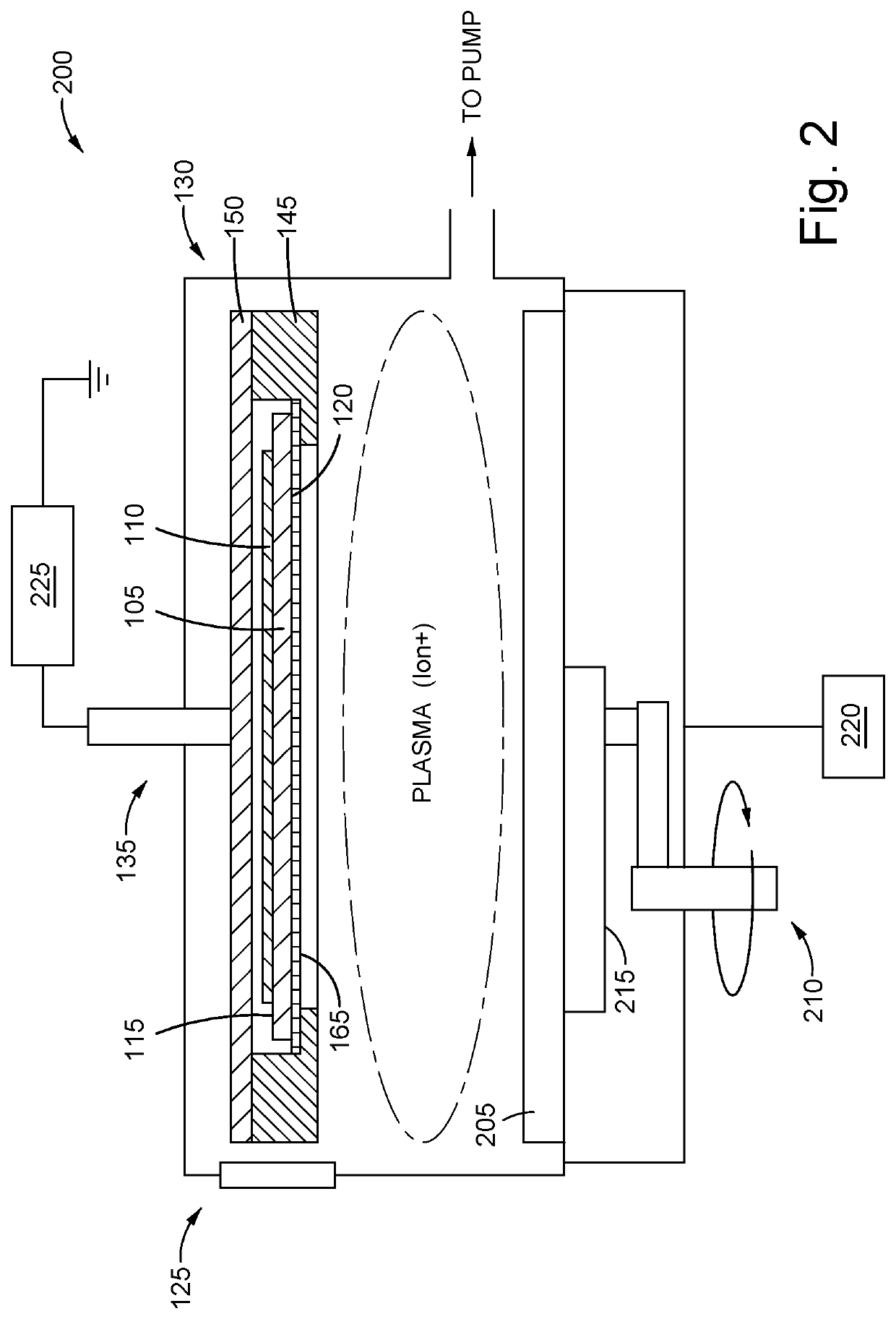
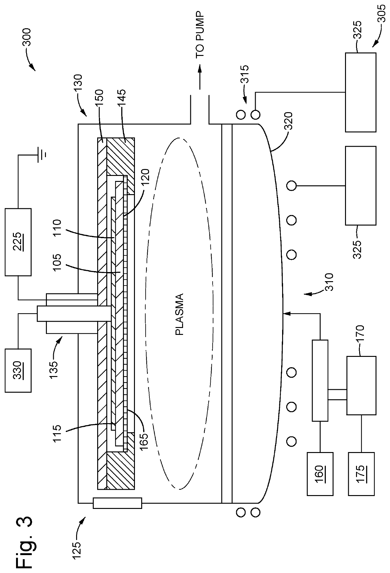
[0024]The present disclosure generally provides a method and apparatus to minimize or control substrate bow or warpage in high density memory device fabrication. The method includes receiving an incoming substrate having a memory film stack formed on a first major surface thereof. The memory film stack includes relatively thick stacks of films, such as multiple oxynitride films, silicon dioxide, silicon nitride and / or polysilicon films. The memory film stack formed on the first major surface of the substrate induces stresses within the substrate that causes the substrate to bow or warp. The bow or warpage creates numerous issues for subsequent processes. The method includes depositing a backside coating onto a second major surface of the substrate. The backside coating includes one or more blanket layers, graded layers, profiled coatings and / or a pattern of one or more films. The backside coating is configured to relieve or counter the stress in the substrate caused by the memory fi...


PUM

PropertyMeasurementUnit
thicknessaaaaaaaaaa
thicknessaaaaaaaaaa
volumeaaaaaaaaaa

Abstract

A method and apparatus for forming a backside coating on a substrate to counteract stresses from a previously deposited film is disclosed. In one embodiment, a method for flattening a bowed substrate includes providing a substrate having a film stack formed on a first major surface thereof, wherein the substrate comprises a bowed orientation, and forming a coating a second major surface of the substrate, wherein the coating is configured to counter stresses produced by the film stack and flattens the substrate from the bowed orientation.

Description

CROSS-REFERENCE TO RELATED APPLICATION[0001]This application claims benefit of United States Provisional Patent Application No. 62 / 736,219, filed Sep. 25, 2018, which is incorporated by reference herein.BACKGROUNDField[0002]Methods and apparatus for semiconductor device processing are disclosed herein. More specifically, embodiments disclosed herein relate to methods and apparatus for elimination of substrate bow or warpage in deposition and patterning high volume manufacturing (HVM) systems.Description of the Related Art[0003]Three dimensional (3D) memory devices, such as 3D NAND, 3D MRAM, etc., have been developed in a variety of configurations that include vertical channel structures. In vertical channel structures, memory cells including charge storage structures are disposed at interface regions between horizontal planes of conductive strips arranged as word lines, and vertical active strips including channels for the memory cells.[0004]The 3D NAND memory product roadmap is bel...

Claims


Application Information

Patent Timeline
Patent Type & Authority Applications(United States)
IPC IPC(8): H01L23/00H01L27/11582H01L21/02C23C16/50C23C14/35C23C14/10C23C14/06C23C16/40C23C16/34C23C16/26
CPCH01L21/02115C23C14/0605H01L27/11582C23C16/26H01L23/562C23C16/402C23C16/345C23C16/50C23C14/0652H01L21/0217C23C14/10H01L21/02164C23C14/35H01L21/56C23C16/44C23C16/042C23C14/22C23C14/042H01L21/302H01L21/02274H01L21/6831C23C14/50C23C16/4585C23C14/044H01J37/321H01J37/32366H10B43/27
Inventor SHENG, SHURANZHANG, LINWERNER, JOSEPH C.
Owner APPLIED MATERIALS INC
Why Eureka
Try Eureka