Microwave photonic vector network analyzer and method for measuring scattering parameters of microwave device

Active Publication Date: 2020-04-02
SHANGHAI JIAO TONG UNIV
View PDF0 Cites 3 Cited by
  • Summary
  • Abstract
  • Description
  • Claims
  • Application Information

AI Technical Summary

Benefits of technology

[0046](1) The present invention uses a photonic sampling technology to receive the signals without superheterodyne structure and/or direct frequency conversion structure, abandons a frequency mixer, a phase-locked loop and a filter, effectively reduces the complexity, size, quality and power consumption of the system,

Problems solved by technology

However, due to the limited bandwidth of an amplitude and phase receiver, high-frequency signals cannot be directly obtained.
A large number of separated elements with complex architecture reduce integration, resulting in a significant increase in price, size, weight, and power consumption.
However, I/Q balance, LO leakage, DC offset, in-band harmonics, 1/f n

Method used


Image

  • Microwave photonic vector network analyzer and method for measuring scattering parameters of microwave device
  • Microwave photonic vector network analyzer and method for measuring scattering parameters of microwave device
  • Microwave photonic vector network analyzer and method for measuring scattering parameters of microwave device

Examples


example 1

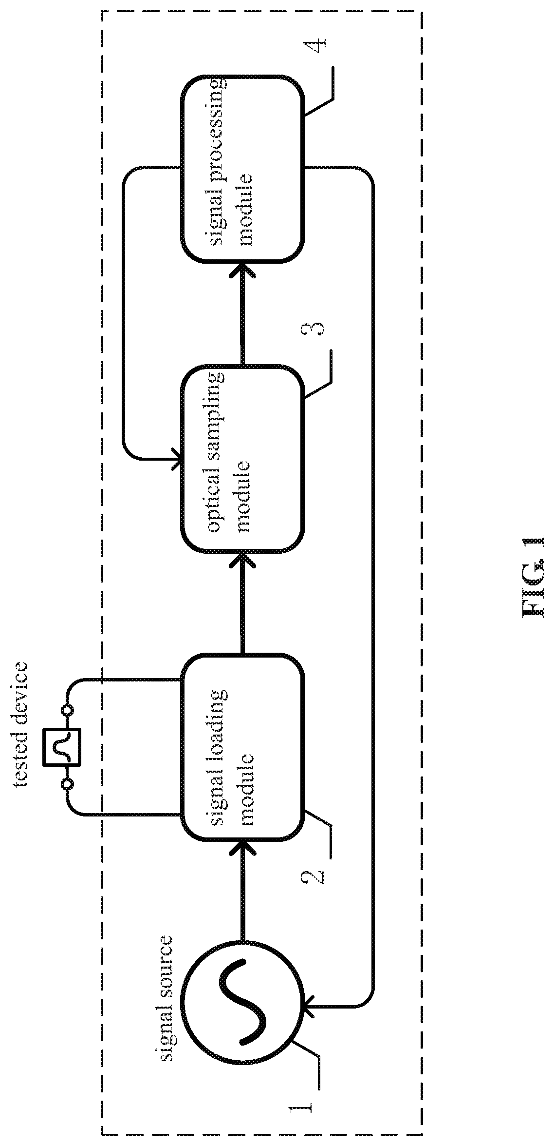
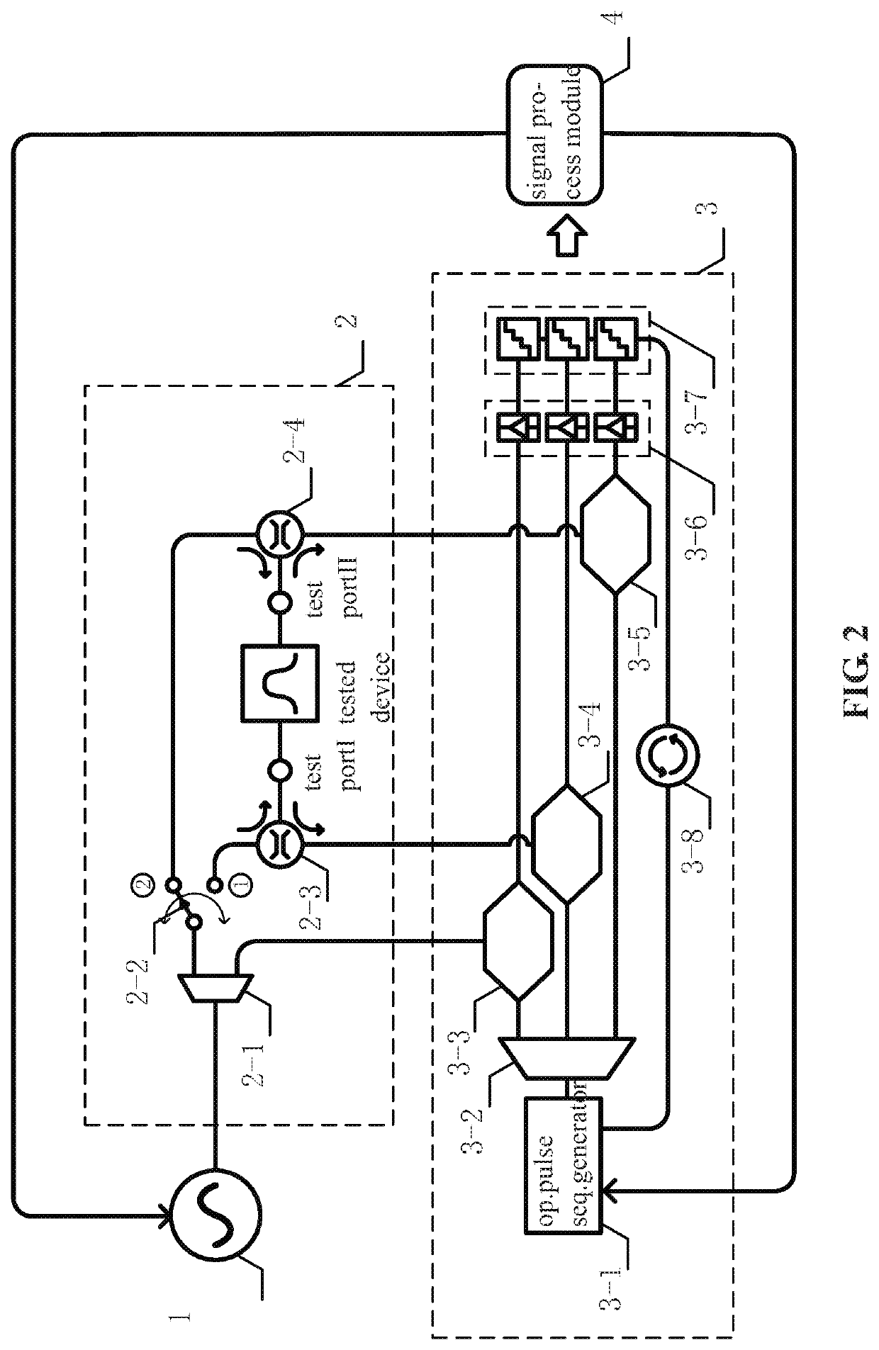
[0052]As shown in FIG. 2, the microwave photonic vector network analyzer of the present invention is a microwave photonic vector network analyzer that comprises a microwave source 1, wherein a signal loading module 2, an optical sampling module 3, and a signal processing module 4 are sequentially arranged along a signal output direction of the microwave source 1; an output end of the signal processing module 4 is respectively connected with a control end of the microwave source 1 and a control end of the optical sampling module 3; and two test ports of the signal loading module 2 are connected with both ends of a device to be tested.

[0053]The signal loading module 2 comprises a power splitter 2-1, a microwave switch 2-2, a first directional coupler 2-3 and a second directional coupler 2-4; and the optical sampling module 3 comprises an optical pulse sequence generator 3-1, an optical coupler 3-2, a reference branch modulator 3-3, a first test branch modulator 3-4, a second test bran...

example 2

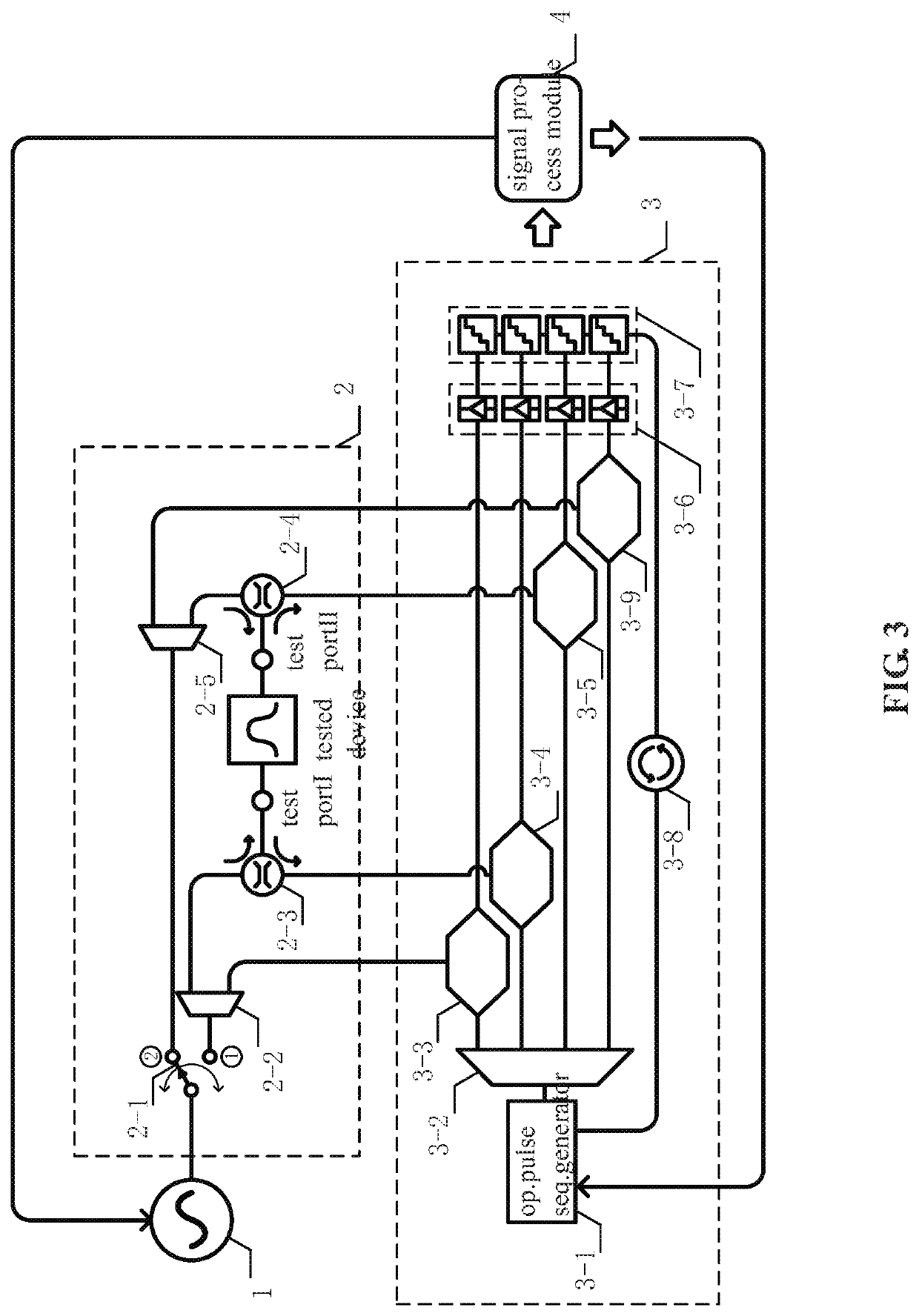
[0070]The system structure is shown in FIG. 3. The system sequentially comprises: a microwave source 1, a signal loading module 2, an optical sampling module 3 and a signal processing module 4, wherein the signal loading module 2 comprises: a microwave switch 2-1, a first power splitter 2-2, a first directional coupler 2-3, a second directional coupler 2-4 and a second power splitter 2-5. The optical sampling module 3 comprises: optical pulse sequence generator 3-1, an optical coupler 3-2, a first reference branch modulator 3-3, a first test branch modulator 3-4, a second test branch modulator 3-5, a second reference branch modulator 3-9, a photoelectric detection module 3-6, an electrical analog-to-digital conversion module 3-7 and a synchronization module 3-8.

[0071]The testing process in the present example comprises the following steps:

[0072](1) setting a test frequency range from fM to fN, and a resolution as Δf; and making fi=fM; (

[0073]2) connecting two ports of the microwave ...


PUM


Abstract

Microwave photonic vector network analyzer and a method for measuring scattering parameters of a microwave device are provided. The analyzer comprises a microwave source, wherein a signal loading module, an optical sampling module and a signal processing module are sequentially arranged along a signal output direction of the microwave source; an output end of the signal processing module is respectively connected with a control end of the microwave source and a control end of the optical sampling module; and two test ports of the signal loading module are connected with both ends of a device to be tested. The invention realizes direct sampling and frequency conversion for microwave signals, abandons a superheterodyne structure and/or direct frequency conversion structure in the traditional network analyzer, simplifies the structure of the system while improving the measurement frequency range and avoiding image interference, and reduces system complexity, cost and power consumption.

Description

CROSS-REFERENCE TO RELATED APPLICATIONS[0001]The subject application is a continuation-in-part of PCT / CN2018 / 114490 filed on Nov. 8, 2018, which in turn claims priority on Chinese Application No. 201810407639.X filed on May 2, 2018 in China. The contents and subject matter of the PCT international application and the Chinese priority application are incorporated herein by reference.TECHNICAL FIELD[0002]The present invention relates to optical information processing technology, particularly, microwave photonic vector network analyzer and method for measuring scattering parameters of a microwave device.BACKGROUND ART[0003]A vector network analyzer is a basic tester in the fields of electronics and communication. It is mainly used to measure scattering parameters of a microwave port network, that is, S parameters. Modern microwave vector network analyzers are greatly improved in many aspects. However, due to the limited bandwidth of an amplitude and phase receiver, high-frequency signa...

Claims


Application Information

Patent Timeline
IPC IPC(8): H04B10/071H04B10/073H04B10/64
CPCH04B10/64H04B10/073H04B10/071G01R27/28H04B10/00H04B10/07H04B10/90H04B2210/006H04B10/40H04B10/50H04B10/60H04B17/30
Inventor WU, GUILINGDING, MINJIN, ZHENGTAO
Owner SHANGHAI JIAO TONG UNIV
Why Eureka
Try Eureka