Semiconductor device and method of manufacturing the same
a technology of semiconductor devices and semiconductor layers, applied in semiconductor devices, semiconductor/solid-state device details, electrical apparatus, etc., can solve the problems of temperature cycling stress and tend to develop cracks in the aluminum layer between the bonding wire and the barrier layer, and achieve the effect of suppressing the propagation of cracks
- Summary
- Abstract
- Description
- Claims
- Application Information
AI Technical Summary
Benefits of technology
Problems solved by technology
Method used
Image
Examples
first embodiment
[0025]Hereinafter, a configuration of a semiconductor device according to a first embodiment will be described.
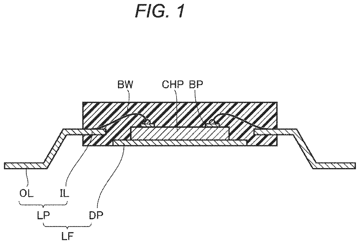
[0026]As shown in FIG. 1, the semiconductor device according to the first embodiment includes a semiconductor chip CHP, bonding wires BW, a lead frame LF, and a sealing resin ER. The semiconductor chip CHP has bonding pads BP. The lead frame LF includes a die pad DP and a lead portion LP. The lead portion LP includes an internal lead IL and an external lead OL. The sealing resin ER is formed of an insulating thermosetting resin such as an epoxy resin, for example.
[0027]The semiconductor chip CHP is mounted on a surface of the die pad DP. The bonding wire BW is connected to the bonding pad BP at one end. The bonding wire BW is connected to the internal lead IL at the other end. The sealing resin ER seals the semiconductor chip CHP, the bonding wire BW, the die pad DP, and the internal leads IL. However, the back surface of the die pad DP is exposed from the sealing resin ER....
second embodiment
[0073]The configuration of a semiconductor device according to a second embodiment will be described below. It should be noted that points different from the configuration of the semiconductor device according to the first embodiment will be mainly described, and description thereof will not be repeated.
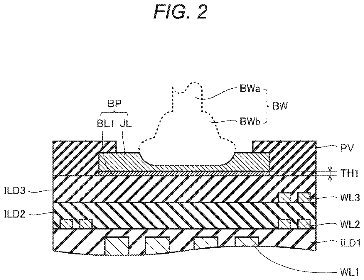
[0074]As shown in FIG. 12, the semiconductor device according to the second embodiment includes a semiconductor chip CHP on which a bonding pad BP is formed and a bonding wire BW. The semiconductor chip CHP includes an interlayer insulating film ILD1, an interlayer insulating film ILD2, an interlayer insulating film ILD3, a wiring WL1, a wiring WL2, and a wiring WL3.
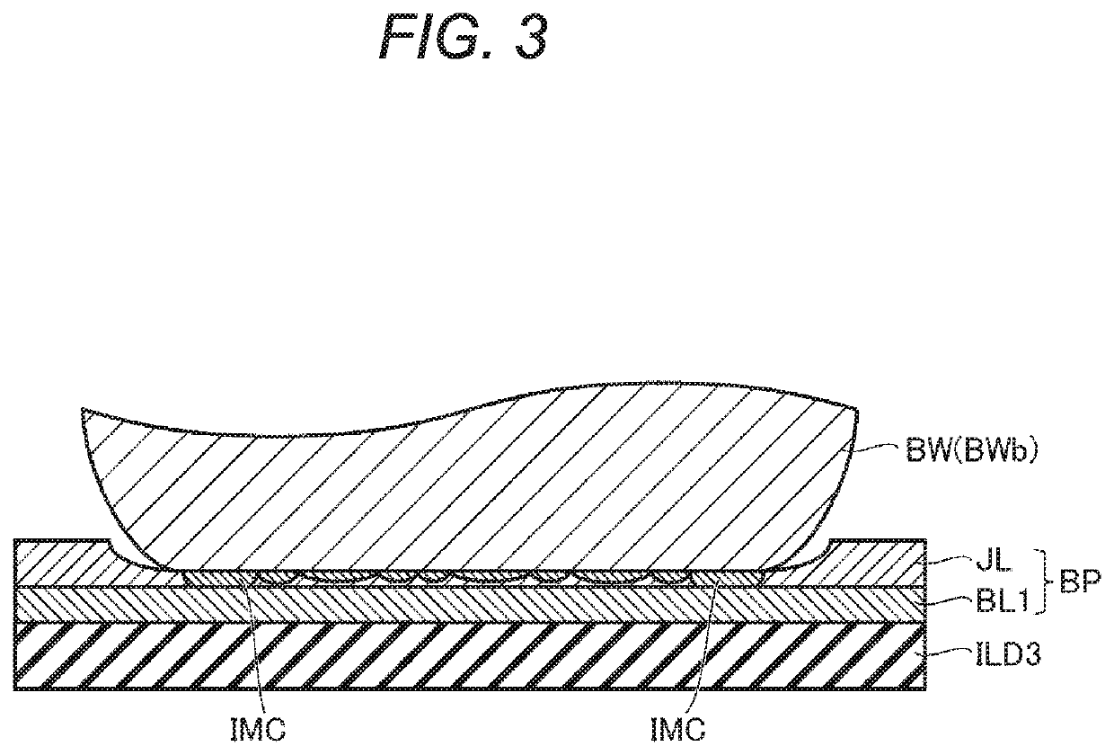
[0075]The bonding pad BP includes a barrier layer BL1 and a bonding layer JL. The intermetallic compound layer IMC is grown from the bonding wire BW to the barrier layer BL1 at least in a portion of a bonding part between the bonding pad BP and the bonding wire BW. In these respects, the configuration of the semiconductor...
third embodiment
[0083]Since a configuration of a semiconductor device according to a third embodiment is the same as that of the semiconductor device according to the first embodiment, detailed description thereof will be omitted. However, in the semiconductor device according to the third embodiment, the wiring WL2 may be arranged so as to overlap with the bonding pads BP in plan view. Further, the wiring WL3 may be disposed so as to overlap the bonding pads BPs in plan view.
[0084]Hereinafter, a method of manufacturing the semiconductor device according to the third embodiment will be described. It should be noted that differences from the manufacturing method of the semiconductor device according to the first embodiment will be mainly described, and description thereof will not be repeated.
[0085]As shown in FIG. 13, the method of manufacturing the semiconductor device according to the third embodiment includes a semiconductor chip preparation step S1 and a bonding step S2. The bonding step S2 inc...
PUM
| Property | Measurement | Unit |
|---|---|---|
| thickness | aaaaa | aaaaa |
| thickness | aaaaa | aaaaa |
| thickness | aaaaa | aaaaa |
Abstract
Description
Claims
Application Information
 - R&D
- Intellectual Property
- Life Sciences
- Materials
- Tech Scout
- Unparalleled Data Quality
- Higher Quality Content
- 60% Fewer Hallucinations
Browse by: Latest US Patents, China's latest patents, Technical Efficacy Thesaurus, Application Domain, Technology Topic, Popular Technical Reports.
© 2025 PatSnap. All rights reserved.Legal|Privacy policy|Modern Slavery Act Transparency Statement|Sitemap|About US| Contact US: help@patsnap.com


