
Sensor Device and Method

a technology of a sensor and a housing, applied in the direction of mechanical control devices, manual control with a single controlling member, instruments, etc., can solve the problems of limited use of certain applications, easy entry of water, dust and other contaminants into the gaps between the control features and the housing, and good longevity and reliability, so as to increase the signal change range in the intended touch area. , the effect of modularity and resolution

Active Publication Date: 2020-06-04
TANGI0 LTD
View PDF0 Cites 3 Cited by
  • Summary
  • Abstract
  • Description
  • Claims
  • Application Information

AI Technical Summary

Benefits of technology

The invention provides a sensor device that can detect touch pressure, speed, and location on the same touch area. This enhances touch control interface performance compared to current devices. The invention simplifies the manufacturing process and reduces production costs. The sensor device has multiple functions simultaneously and avoids multiple molding processes. The invention also includes an insulating barrier that allows for sensing modularity and resolution, and a computer program that can detect touch location, movement direction, and pressure or force.

Problems solved by technology

However, they suffer a number of drawbacks.
For example, they are predominantly flat and rigid, which limits their use in certain applications.
Furthermore, where any buttons, joysticks, keys etc. are provided on / in the controller housing, the gaps between the control features and the housing are prone to entry by water, dust and other contaminants.
Certain applications in particular, for example automotive interiors, require good longevity and reliability, and any gaps could permit such contaminants to enter and lead to failure of the electronic circuits housed inside.
Where steps have been taken to address the problem, this has inevitably led to increased costs and complexities.
This is often undesirable, particularly in mass produced, low value electronic items and in a commercial marketplace that is already busy and competitive.
A filler or other protective material would need to be provided between the foam and printed circuitry, but this would increase manufacturing and shipping costs, as well as increasing raw material demands.
This would also necessitate multiple moulding processes during manufacture, leading to said undesirable increased manufacturing costs.

Method used


Image

  • Sensor Device and Method
  • Sensor Device and Method
  • Sensor Device and Method

Examples


Embodiment Construction

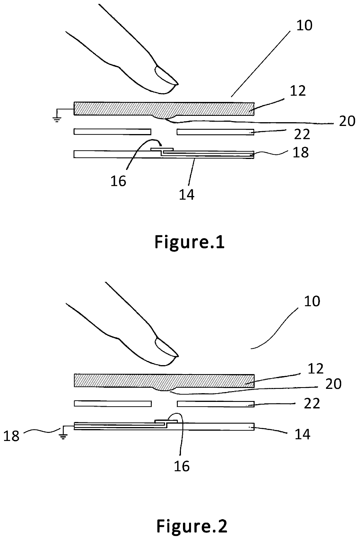
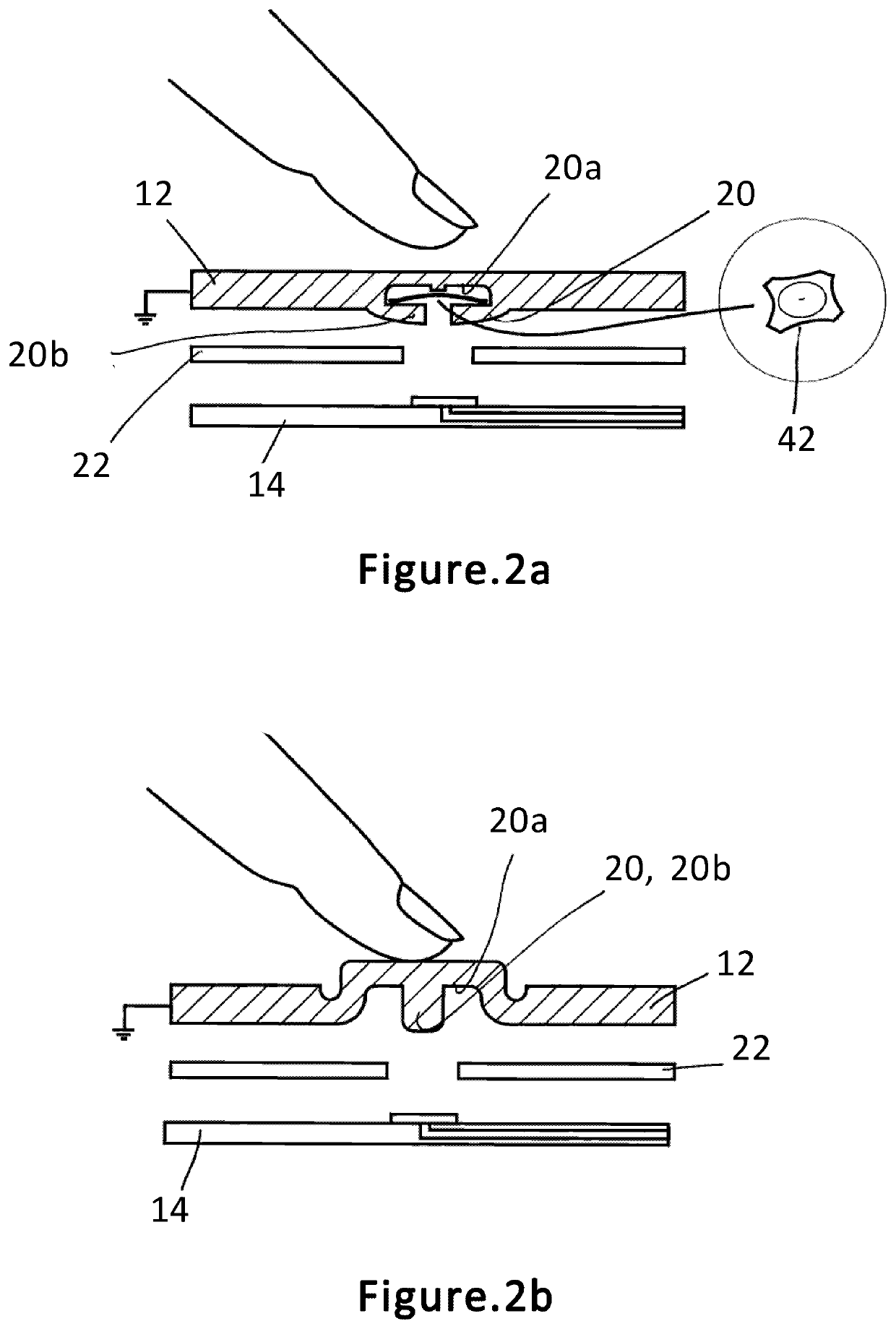
[0067]FIG. 1 shows a sensor device or user interactive element 10. The sensor device 10 comprises a layer or portion of electrically conductive material 12. The sensor device also has a circuitry layer 14 and a barrier, preferably in the form of a separation or isolation layer 22 between the layer of electrically conductive material and the circuitry layer. The whole device 10 can be configured to fit in or on top of an existing counter-part, e.g. a car interior door panel (as shown in FIG. 21, discussed below). It is to be appreciated that whilst it is necessary for the conductive layer 12 to be adjacent to the separation layer 22 and for that to be adjacent to the circuitry layer 14, these need not be flat layers.

[0068]The conductive layer 12 is provided in the form of a generally planar sheet 12. The conductive material 12 is pliable, deformable and / or flexible. The conductive material 12 may be formed of a silicone rubber containing conductive material such as conductive metal p...


PUM

PropertyMeasurementUnit
thicknessaaaaaaaaaa
electricalaaaaaaaaaa
electrically conductiveaaaaaaaaaa

Abstract

A sensor device has a plurality of electrode portions configured to provide one or more electrical signals and a non-conductive material provided on or over the plurality of electrode portions. The one or more electrical signals are provided in response to a change in capacitance between (i) at least one of the plurality of electrode portions and a conductive object being near to or in contact with the non-conductive material, and / or (ii) at least one of the plurality of electrode portions and at least one other of the plurality of electrode portions. A system comprising the sensor device and method of manufacturing the sensor device are also provided.

Description

TECHNICAL FIELD[0001]The present invention relates to a sensor device and, in particularly but not exclusively, to a sensor that can perform both analogue touch location sensing and digital pressure / force sensing.BACKGROUND TO THE INVENTION[0002]Tactile sensors provide a way of obtaining information via a physical interaction with the sensor, and are commonly used in applications such as mobile and computing devices, robotics, and control systems. These may operate based on piezoresistive, piezoelectric, capacitive and elastoresistive sensing. For example, in a capacitive touch switch, a person needs merely to touch the sensor, which changes the capacitance within the sensor and triggers the switch. A variety of pressure sensitive materials are now available, including quantum tunneling composites, for use in pressure switching and sensing. These are utilized in soft robotics, heavy machinery and wearables. Examples including conductive inks have been developed to integrate sensitiv...

Claims


Application Information

Patent Timeline
Patent Type & Authority Applications(United States)
IPC IPC(8): G06F3/044G06F3/045
CPCG06F2203/04104G06F3/0447G06F3/045H01H13/704G06F3/0443G06F3/0446G06F2203/04108G06F3/0416G01L1/20G05G9/047G06F3/0338G06F3/03547G06F3/0414H01H25/041
Inventor LIN, CHIA-HUNGCORREA, ILAN JOHAN EDUARDO OLIVAREZGUO, LIUCHENGKONG, MING
Owner TANGI0 LTD
Learn More