Electrostatic discharge protection device

a protection device and electrostatic discharge technology, applied in semiconductor devices, diodes, transistors, etc., can solve problems such as undesired timing of esd protection devices

Active Publication Date: 2020-06-18
SK HYNIX INC
View PDF0 Cites 3 Cited by
  • Summary
  • Abstract
  • Description
  • Claims
  • Application Information

AI Technical Summary

Benefits of technology

[0010]In example embodiments of the present invention disclosure, an electrostatic discharge (ESD) protection device may include a gate, a source, a diode, a first peripheral well and a boundary region. The gate is formed over an active well. The source and a drain are formed in the active well on either side of the gate. The diode region is formed in the active well adjacent and in contact with the drain. The first peripheral well is formed under the...

Problems solved by technology

When an ESD protection device having a holding voltage that is lower than the operational voltage is used, ESD stresses may be generated in operating the semiconductor integrated circuit device which may result in the ESD protection device operati...

Method used


Image

  • Electrostatic discharge protection device
  • Electrostatic discharge protection device
  • Electrostatic discharge protection device

Examples


Embodiment Construction

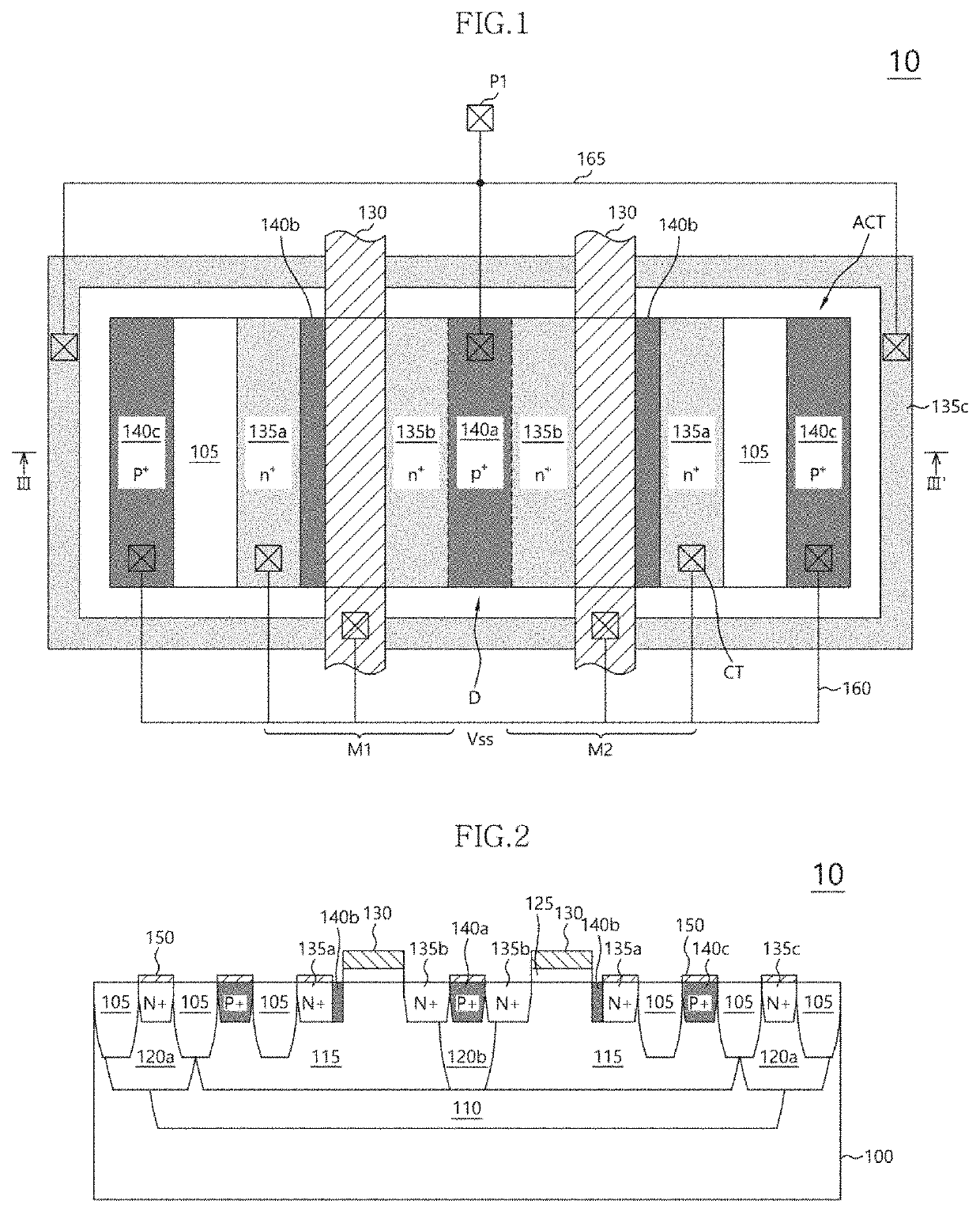
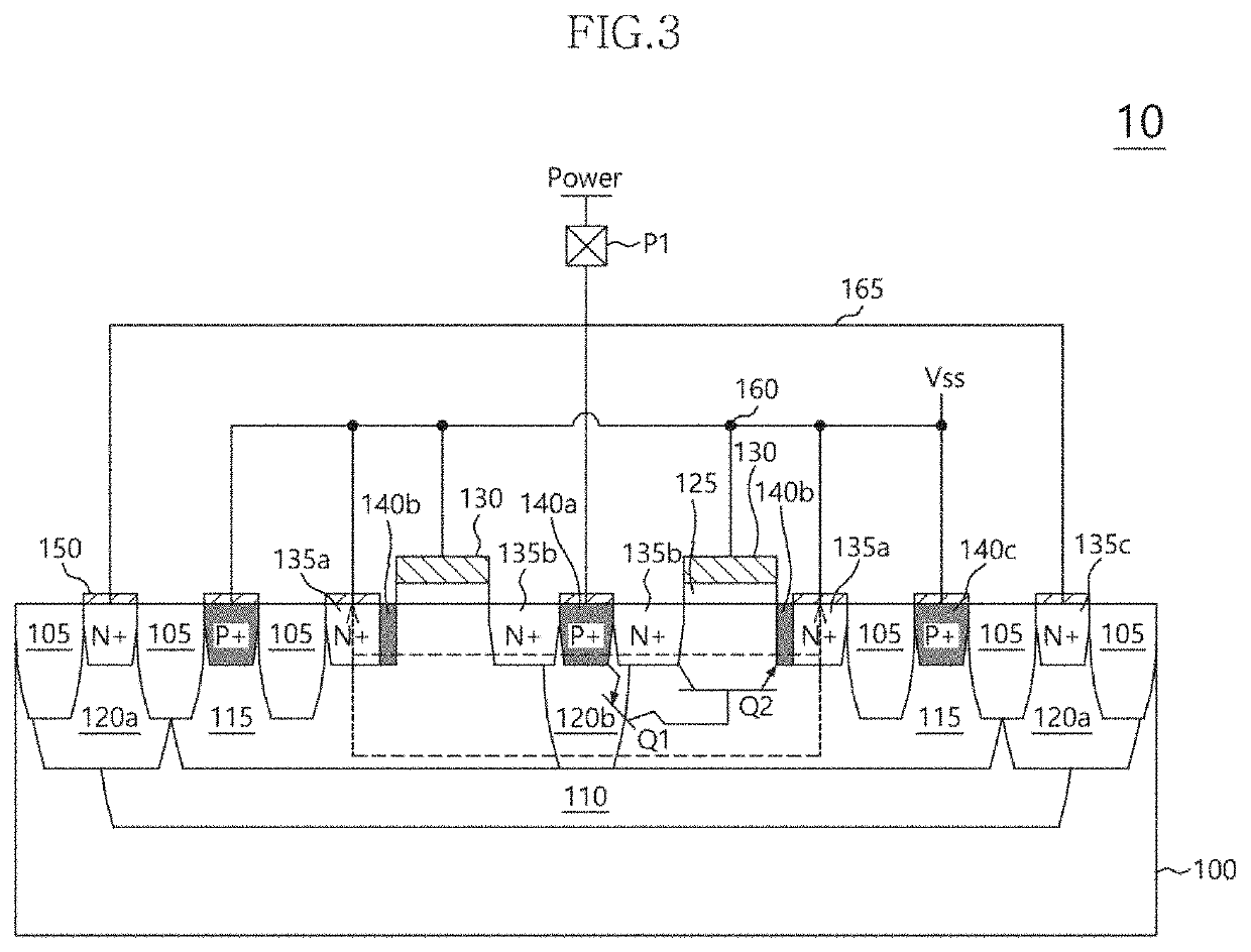
[0020]Various embodiments of the present invention will be described in greater detail with reference to the accompanying drawings. The drawings are schematic illustrations of various embodiments (and intermediate structures). As such, variations from the configurations and shapes of the illustrations as a result, for example, of manufacturing techniques and / or tolerances, are to be expected. Thus, the described embodiments should not be construed as being limited to the particular configurations and shapes illustrated herein but may include deviations in configurations and shapes which do not depart from the spirit and scope of the present invention as defined in the appended claims.

[0021]The present invention is described herein with reference to cross-section and / or plan illustrations of idealized embodiments of the present invention. However, embodiments of the present invention should not be construed as limiting the inventive concept. Although a few embodiments of the present ...


PUM


Abstract

An electrostatic discharge (ESD) protection device includes a pad, a diode, a gate ground NMOS (GGNMOS) transistor and a thyristor. The diode includes an anode connected with the pad. The GGNMOS transistor is connected between a cathode of the diode and a ground terminal. The thyristor is formed between the diode and the ground terminal when an ESD current may flow from the pad.

Description

CROSS-REFERENCES TO RELATED APPLICATION[0001]The present application claims priority under 35 U.S.C. § 119(a) to Korean application number 10-2018-0163140, filed on Dec. 17, 2018, which is incorporated herein by reference in its entirety.BACKGROUND1. Technical Field[0002]Various embodiments of the present invention generally relate to a semiconductor integrated circuit device and, more particularly, to an electrostatic discharge (ESD) protection device.2. Related Art[0003]A semiconductor integrated circuit device may include an electrostatic discharge (ESD) protection device for protecting an internal circuit. Typically, the ESD protection device is arranged between the internal circuit and a pad for receiving an external signal. An ESD protection device may have a MOS transistor structure, a silicon controlled rectifier (SCR) structure, etc.[0004]Generally, an ESD protection device having the SCR structure may have a bypass capacity of an ESD stress current superior to that of an E...

Claims


Application Information

Patent Timeline
IPC IPC(8): H01L27/02H02H9/04
CPCH01L27/0277H01L27/0255H01L27/0288H01L27/0292H02H9/046H01L27/0262H01L27/0274H01L29/7404H01L29/7408
Inventor CHOI, JOUNG CHEULSONG, CHANG SEOK
Owner SK HYNIX INC
Why Eureka
Try Eureka