Packaging of a directly modulated laser chip in photonics module

a technology of photonic modules and laser chips, applied in semiconductor lasers, optical elements, instruments, etc., can solve the problems of serial link performance being limited by electrical bandwidth and electronic components of channels, affecting the performance of serial links, and continuously requiring a huge amount of bandwidth for transferring photos, video, music, etc., to achieve the effect of eliminating unwanted noise sources and increasing the transmitter bandwidth

Active Publication Date: 2020-06-18
MARVELL ASIA PTE LTD
View PDF0 Cites 2 Cited by
  • Summary
  • Abstract
  • Description
  • Claims
  • Application Information

AI Technical Summary

Benefits of technology

[0013]Therefore, the present disclosure has at least following advantages. First, the package structure for coupling a galvanically coupled output of a flip-chip driver to a directly modulated laser (DML) chip in a photonics transceiver module substantially increasing the transmitter bandwidth without wirebond to eliminate unwanted noise source due to parasitic inductance. Secondly, the DML chip used in the photonics transceiver module can be advantageously made with a common-electrode configuration.

Problems solved by technology

But Internet and mobile applications continuously demand a huge amount of bandwidth for transferring photo, video, music, and other multimedia files.
Serial link performance is limited by the channel electrical bandwidth and the electronic components.
Stacking chips into so-called 3-D ICs promises a one-time boost in their capabilities, but it's very expensive.

Method used


Image

  • Packaging of a directly modulated laser chip in photonics module
  • Packaging of a directly modulated laser chip in photonics module
  • Packaging of a directly modulated laser chip in photonics module

Examples


Embodiment Construction

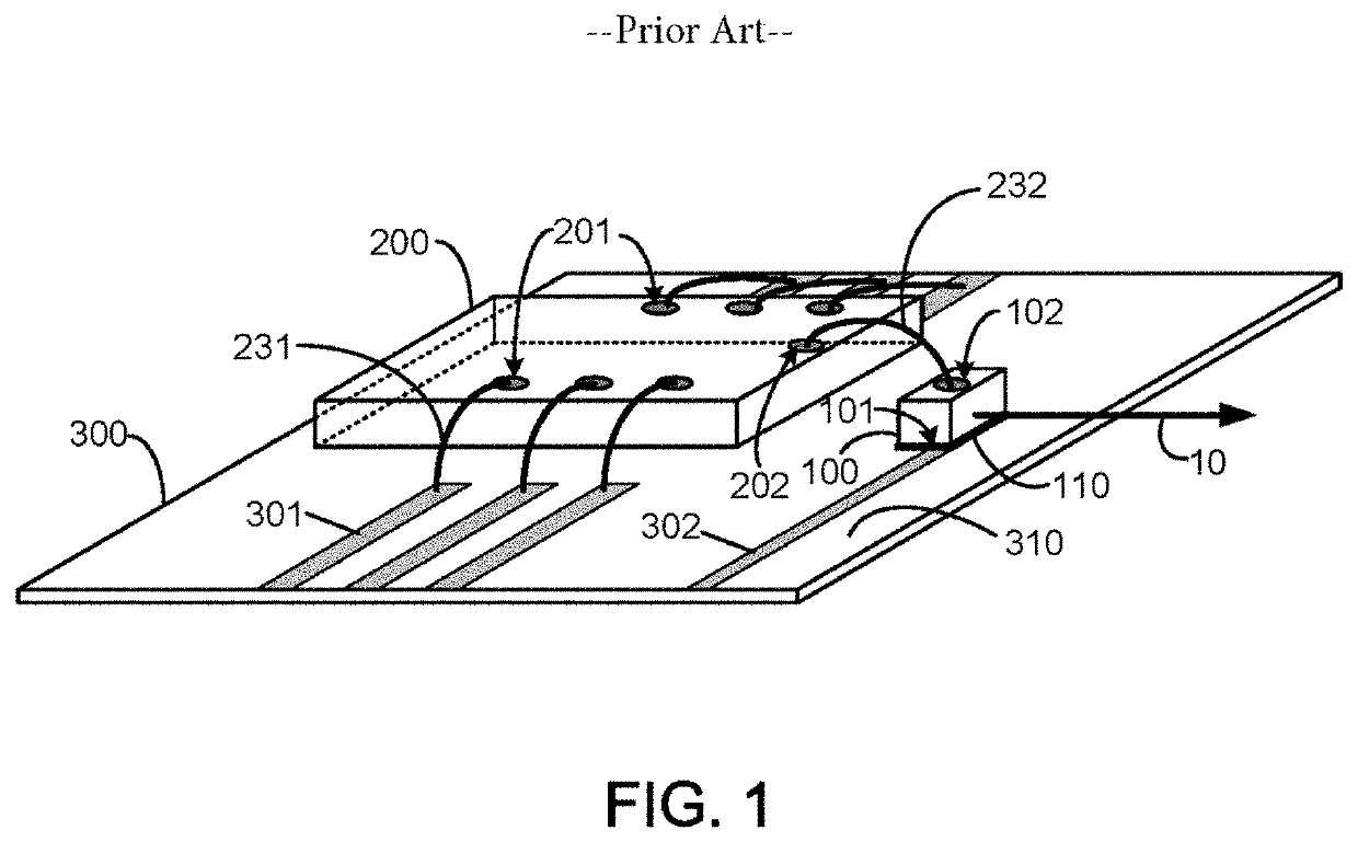
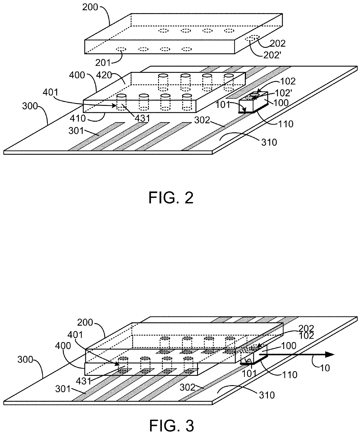
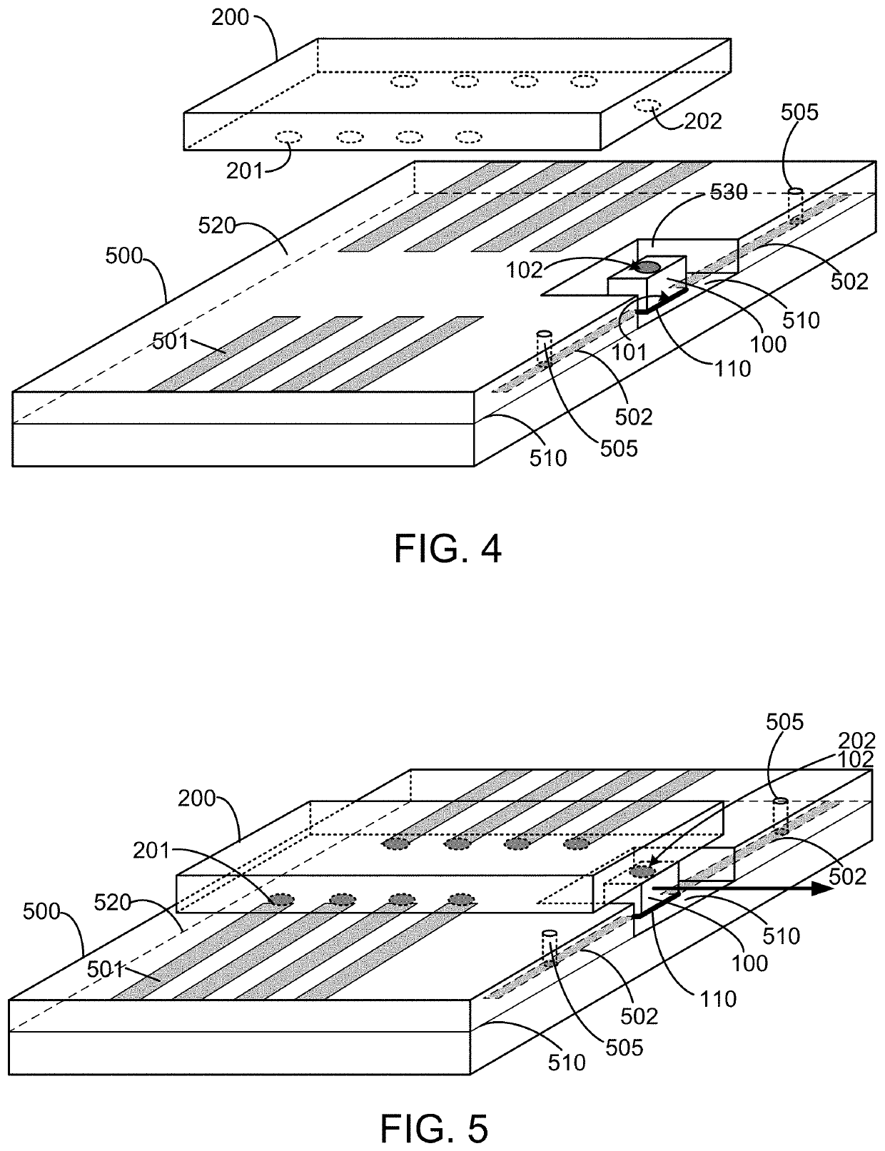
[0023]The present disclosure is related to a photonic package structure, more particularly, to a package structure for disposing a flip-chip driver directly on a substrate or via an interposer with a galvanically coupled output directly connected to a directly modulated laser (DML) chip in a photonics transceiver module. In certain embodiments, the invention is applied for packaging photonics module for high data-rate optical communication. For example, the DML chip is installed in a TEC-TOSA laser device in a pluggable photonic transceiver in Quad Small Form-factor Pluggable (QSFP) packaging specification. Other applications are possible.

[0024]The following description is presented to enable one of ordinary skill in the art to make and use the invention and to incorporate it in the context of particular applications. Various modifications, as well as a variety of uses in different applications will be readily apparent to those skilled in the art, and the general principles defined ...


PUM

PropertyMeasurementUnit
electrical signalsaaaaaaaaaa
thermal conductiveaaaaaaaaaa
distanceaaaaaaaaaa

Abstract

A package structure of a directly modulated laser in a photonics module includes a thermoelectric cooler including multiple conductor traces formed in a cool surface. The package structure further includes a directly modulated laser (DML) chip having a first electrode being attached with the cool surface and a second electrode at a distance away from the cool surface. Additionally, the package structure includes an interposer having a plurality of through-holes formed between a first surface to a second surface. The first surface is mounted to the cool surface such that each through-hole is aligned with one of the multiple conductor traces and the second surface being leveled with the second electrode. Moreover, the package structure includes a driver disposed on the second surface of the interposer with at least a galvanically coupled output port coupled directly to the second electrode of the DML chip.

Description

CROSS-REFERENCE TO RELATED APPLICATIONS[0001]This application is a continuation of and claims priority to U.S. application Ser. No. 15 / 896,955, filed Feb. 14, 2018, commonly assigned and incorporated by reference herein for all purposes.BACKGROUND OF THE INVENTION[0002]The present disclosure is related to a photonic package structure, more particularly, to a package structure for disposing a flip-chip driver directly on a substrate or via an interposer to have a galvanically coupled output directly connected to a directly modulated laser (DML) chip with minimized inductance in a photonics transceiver module.[0003]As science and technology are progressing rapidly, processing speed and capacity of the computer increase correspondingly. The communication transmission or reception using the traditional cable is limited to bandwidth and transmission speed of the traditional cable, but the mass information transmission required in modern life causes the traditional communication transmiss...

Claims


Application Information

Patent Timeline
Patent Type & Authority Applications(United States)
IPC IPC(8): H01S5/024G02B6/42H01S5/022H05K1/02H04B10/50H01S5/0233
CPCH01S5/0226H01S5/02415H01S5/0224G02B6/4266H04B10/504H05K1/0204H01S5/04256H01S5/06226H04B10/58G02B6/4271H01S5/023H01S5/0233H01S5/0235H01S5/02325H01S5/02345H01S5/0234H01S5/0236
Inventor GELHAUSEN, FRANKAHMED AWNY, AHMED SANAAPILLAI, EDWARDSCHACHT, ULRICHPIEPENSTOCK, OLIVER
Owner MARVELL ASIA PTE LTD
Why Eureka
Try Eureka