

Memory system and operation method thereof
a memory system and operation method technology, applied in the field of error detection and correction, can solve the problems of additional errors, difficult to fabricate a memory device with no defective memory cells, and the very unlikely that such a defect-free memory device will be fabricated, so as to improve the efficiency of error detection and error correction
- Summary
- Abstract
- Description
- Claims
- Application Information
AI Technical Summary
Benefits of technology
Problems solved by technology
Method used
Image

Examples
Embodiment Construction
[0016]Various embodiments of the present invention are described below in more detail with reference to the accompanying drawings. The present invention may, however, be embodied in other forms and thus should not be construed as limited to the embodiments set forth herein. Rather, these embodiments are provided so that this disclosure is thorough and complete and fully conveys the scope of the present invention to those skilled in the art. Throughout the disclosure, like reference numerals refer to like parts throughout the various figures and embodiments of the present invention. Also, throughout the specification, reference to “an embodiment,”“another embodiment” or the like is not necessarily to the same embodiment, and different references to any such phrase are not necessarily to the same embodiment(s).
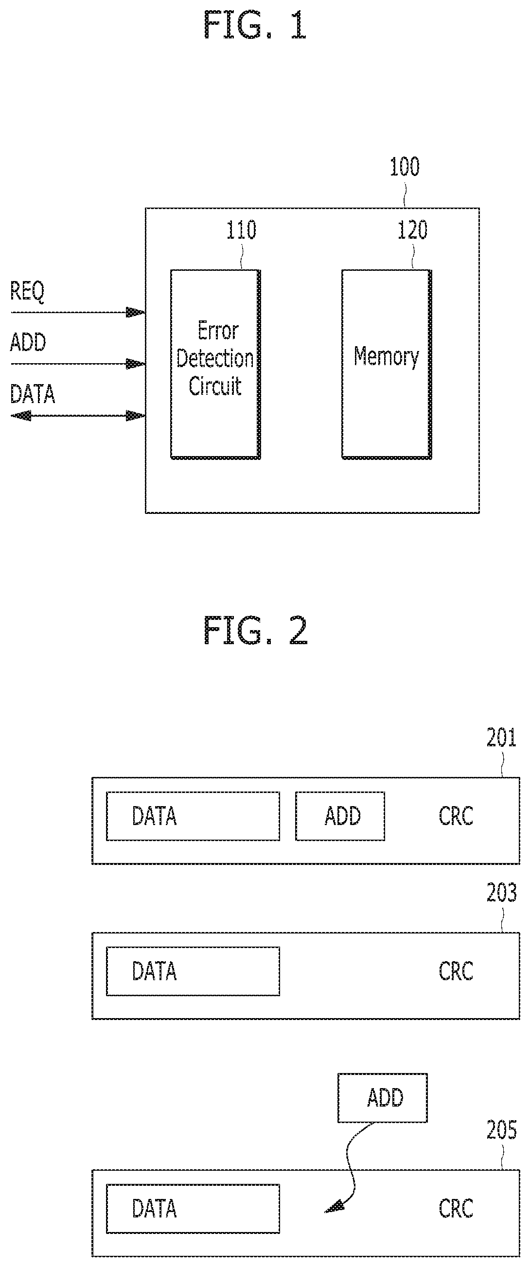
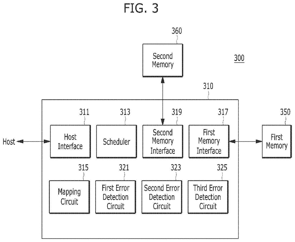
[0017]FIG. 1 is a diagram illustrating a memory system 100 in accordance with an embodiment.
[0018]Referring to FIG. 1, the memory system 100 may include an error detection circu...
PUM
 Abstract
Description
Claims
Application Information