Deterministic Quantum Emitter Formation in Hexagonal Boron Nitride via Controlled Edge Creation

a boron nitride and quantum emitter technology, applied in the field of solid-state optical devices, can solve the problems of limiting the viability of widespread use, complex setup, and no method for deterministically and reliably fabricating qes in hbn at desired locations in a manner, and achieves the effect of broadening the utility and convenience of hbn qes and specific size and shap

Active Publication Date: 2020-08-13
UNIVERSITY OF OREGON
View PDF0 Cites 4 Cited by
  • Summary
  • Abstract
  • Description
  • Claims
  • Application Information

AI Technical Summary

Benefits of technology

[0006]The inventors have discovered a method to deterministically create QEs at controlled locations in hBN. QEs are fabricated by creating edges having specific characteristics, e.g., using patterned milling of holes in hBN using a gallium focused ion beam (FIB). Through the use of specific milling and annealing parameters, a 31% yield of single QEs was achieved. It was discovered that the QEs form best and with preferably properties through uniform milling of smooth holes on relatively smooth chemical vapor deposition (CVD) hBN. The result of this method is a fabricated QE nanoscale device with specific size and shape characteristics. Also provided are arrays of such QEs. Optical confocal microscopy confirmed that such an array exhibits an array of bright, localized photoluminescence that match the geometry of the patterned holes. Second-order photon correlation measurements on these bright spots confirm that they contain single and multiple QEs. This technique dramatically broadens the utility and convenience of hBN QEs and achieves a vital step toward the facile integration of the QEs into large-scale photonic, plasmonic, nanomechanical, or optoelectronic devices.

Problems solved by technology

However, the more commonly used quantum emitters (QEs), such as cold atoms and spontaneous parametric down-conversion sources, require complex setups that limit their viability for widespread use.
However, no method exists for deterministically and reliably fabricating QEs in hBN at desired locations in a manner suitable for integration with hybrid quantum devices.

Method used


Image

  • Deterministic Quantum Emitter Formation in Hexagonal Boron Nitride via Controlled Edge Creation
  • Deterministic Quantum Emitter Formation in Hexagonal Boron Nitride via Controlled Edge Creation
  • Deterministic Quantum Emitter Formation in Hexagonal Boron Nitride via Controlled Edge Creation

Examples


examples

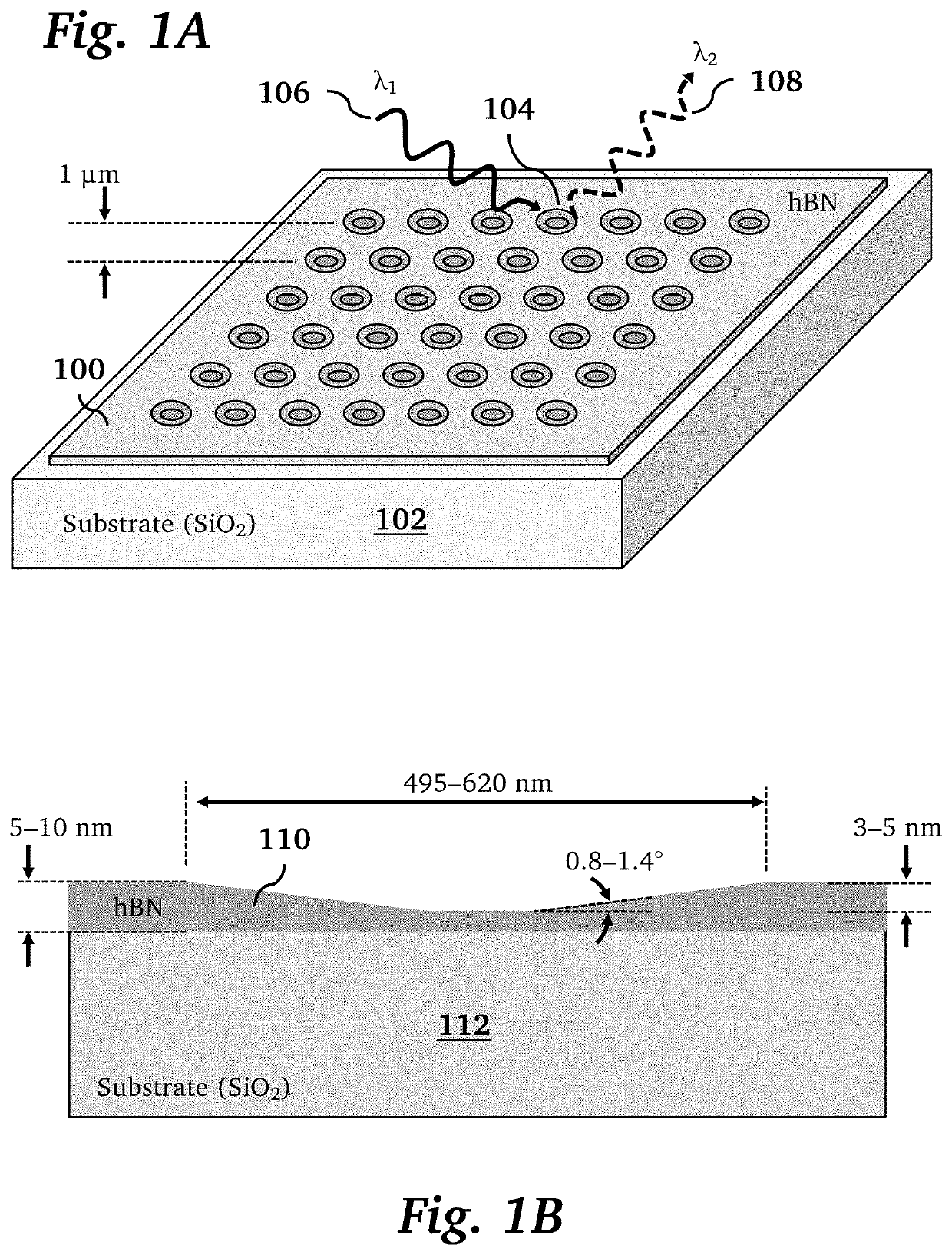
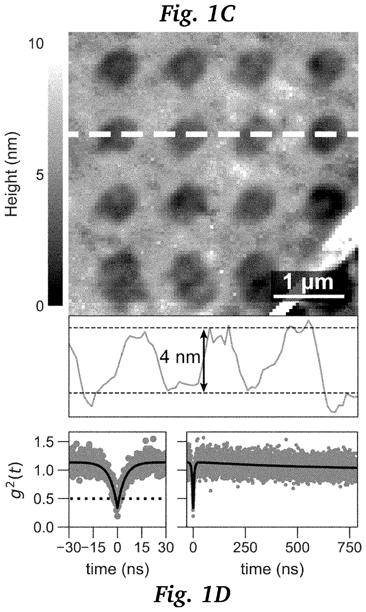
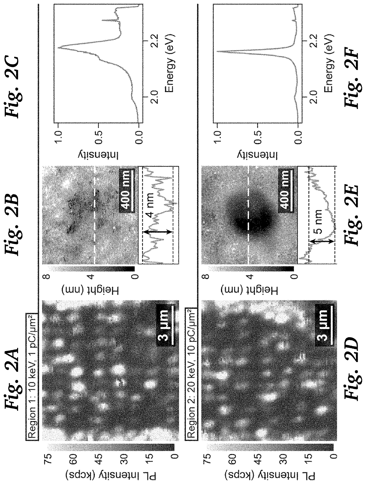
[0042]To create QEs in our hBN via edge creation, we transfer few-layer CVD hBN (Graphene Supermarket) onto SiO2 and then use FIB to mill holes into the hBN, thereby forming edges at the hole perimeter. We do not perform an additional irradiation to activate QEs. The required dose to remove hBN material was in the range 10−13 C / μm2 to 10−10 C / μm2, with beam energies from 5 to 30 keV. Initial tests showed that energies of either 10 or 20 keV and milling doses of 1pC / μm2 were close to optimum for QE creation, as inferred by g2(0)2, while in another region (Region 2) we used 20 keV and 10 pC / μm2. To generate a high density of single, optically addressable QEs with enough perimeter for QEs to form, we FIB patterned arrays of 500 nm diameter circular holes with a center-to-center separation of 1 μm in each region. An atomic force microscope (AFM) image of these holes is shown in FIG. 1C, with a line cut shown below. The FIB was operated at 20 keV and 10 pC / μm2. The depth of the holes for...


PUM

PropertyMeasurementUnit
side wall angleaaaaaaaaaa
depthaaaaaaaaaa
thicknessaaaaaaaaaa

Abstract

A quantum emitter device is composed of a hole milled in a layer of hexagonal boron nitride (hBN) on a substrate made of silicon dioxide. The hole preferably has a side wall angle 1.1°±0.28° from the horizontal, has an oval shape with minor axis 516 nm±20 nm and major axis 600 nm±20 nm, and / or has a depth 4 nm±1 nm. The hBN layer preferably has a total thickness of 5-10 nm. The holes may be fabricated using a gallium focused ion beam, a helium focused ion beam, electron beam directed etching, or photolithography and reactive ion etch (RIE) with sidewall tapering.

Description

CROSS-REFERENCE TO RELATED APPLICATIONS[0001]This application claims priority from U.S. Provisional Patent Application 62 / 804,535 filed Feb. 12, 2019, which is incorporated herein by reference.STATEMENT REGARDING FEDERALLY SPONSORED RESEARCH OR DEVELOPMENT[0002]This invention was made with Government support under contract DMR-1532225 awarded by the National Science Foundation. The Government has certain rights in the invention.FIELD OF THE INVENTION[0003]The present invention relates generally to solid state optical devices. More specifically, it relates to the quantum emitters and their fabrication.BACKGROUND OF THE INVENTION[0004]Sources of single photons are a key component of many emerging quantum information technologies such as quantum computation, communication, and sensing. However, the more commonly used quantum emitters (QEs), such as cold atoms and spontaneous parametric down-conversion sources, require complex setups that limit their viability for widespread use. In con...

Claims


Application Information

Patent Timeline
Patent Type & Authority Applications(United States)
IPC IPC(8): H01L39/12
CPCG06N10/00H04B10/70H04B10/291H01L39/12G06E3/005H01L33/06H01L33/32H01L33/26B82Y20/00H10N60/85
Inventor ALEMÁN, BENJAMÍN J.ZIEGLER, JOSHUA E.
Owner UNIVERSITY OF OREGON
Why Eureka
Try Eureka