Piezoelectric element, liquid ejecting head, and printer

a liquid ejecting head and piezoelectric layer technology, applied in the direction of piezoelectric/electrostrictive/magnetostrictive devices, printing, electrical equipment, etc., can solve the problems of difficult to accurately identify the crystal structure of a thin film piezoelectric layer, easy cracking, and increased leakage current, etc., to achieve the effect of simplifying explanation

Active Publication Date: 2020-08-27
SEIKO EPSON CORP
View PDF0 Cites 0 Cited by
  • Summary
  • Abstract
  • Description
  • Claims
  • Application Information

AI Technical Summary

Benefits of technology

[0008]Regarding plane orientation, the crystal structure of the piezoelectric layer is assumed to be pseudo-cubic. This is for the sake of simplifying explanation because it is difficult to accurately identify the crystal structure of a thin film piezoelectric layer. However, regarding the plane orientation, even though the crystal structure of the piezoelectric layer is assumed to be pseudo-cubic, the crystal structure of the piezoelectric layer may be an ABO3 structure such as tetragonal, orthorhombic, monoclinic, or rhombohedral that is less symmetric than pseudo-cubic. For example, when the crystal structure of the piezoelectric layer is tetragonal, (100) orientation refers to both (001) orientation and (100) orientation.

Problems solved by technology

When the piezoelectric layer is not oriented, cracking may readily occur in the piezoelectric layer, or a leakage current may increase.
This is for the sake of simplifying explanation because it is difficult to accurately identify the crystal structure of a thin film piezoelectric layer.

Method used


Image

  • Piezoelectric element, liquid ejecting head, and printer
  • Piezoelectric element, liquid ejecting head, and printer
  • Piezoelectric element, liquid ejecting head, and printer

Examples


example 1

5.1.1. Example 1

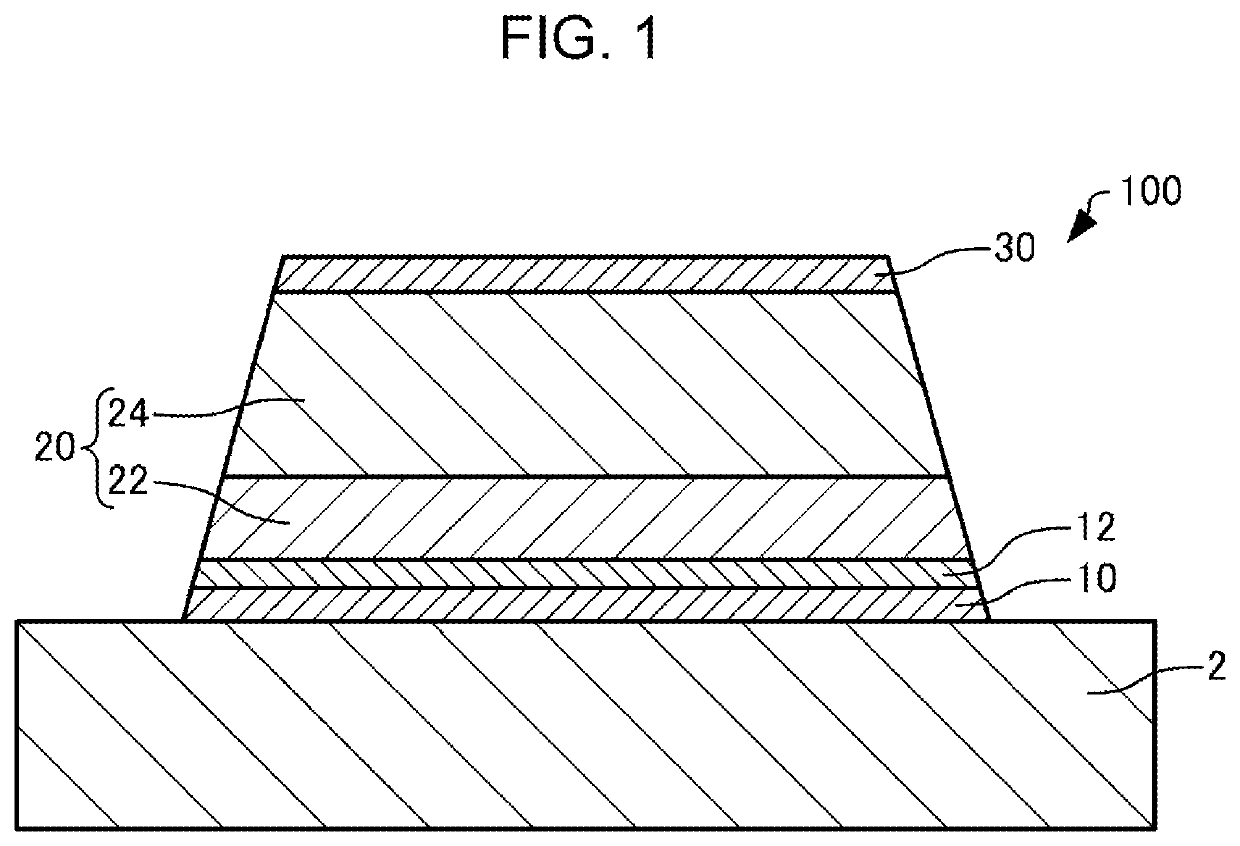
[0082]In Example 1, a silicon dioxide layer was formed on a silicon substrate by thermally oxidizing a 6-inch silicon substrate. A zirconium layer was formed on the silicon dioxide layer by a sputtering method, and a zirconium oxide layer was formed by performing thermal oxidation. A titanium layer, a platinum layer, an iridium layer, and a titanium layer were formed in this order on the zirconium oxide layer by the sputtering method to form an adhesive layer composed of a titanium layer, a first electrode composed of the platinum layer and the iridium layer, and an orientation-control layer composed of the titanium layer.

[0083]A piezoelectric layer was formed on the orientation control layer in the following procedure.

[0084]Acetic acid and water were measured and taken into a container, and lead acetate, zirconium butoxide, titanium tetra-i-propoxide, and polyethylene glycol were also measured and taken into the container. These were heated and agitated at 90° C. to...


PUM

PropertyMeasurementUnit
crystal structureaaaaaaaaaa
piezoelectricaaaaaaaaaa
liquid ejectingaaaaaaaaaa

Abstract

A piezoelectric element includes a first electrode disposed at a base body, a second electrode, and a piezoelectric layer disposed between the first electrode and the second electrode. The piezoelectric layer includes a first piezoelectric layer containing a complex oxide having a perovskite structure that contains lead, zirconium, and titanium and a second piezoelectric layer containing a complex oxide having a perovskite structure that is denoted by formula (1) below. The first piezoelectric layer is disposed between the first electrode and the second piezoelectric layer and is preferentially oriented to (100) when the crystal structure of the first piezoelectric layer is assumed to be pseudo-cubic,
xPb(Mg,Nb)O3-yPbZrO3-zPbTiO3  (1)
where in formula (1), 0<x,y,z<1 and x+y+z=1.

Description

[0001]The present application is based on, and claims priority from JP Application Serial Number 2019-032592, filed Feb. 26, 2019, the disclosure of which is hereby incorporated by reference herein in its entirety.BACKGROUND1. Technical Field[0002]The present disclosure relates to a piezoelectric element, a liquid ejecting head, and a printer.2. Related Art[0003]Typical examples of the liquid ejecting head include ink jet recording heads in which ink in a pressure generation chamber is pressurized by a vibrating plate deformed by a piezoelectric element and is ejected as ink droplets through a nozzle hole.[0004]Examples of the piezoelectric element usable for ink jet recording heads include piezoelectric elements formed by interposing, between two electrodes, a piezoelectric material having an electromechanical conversion function, for example, a piezoelectric layer composed of a crystallized dielectric material.[0005]For example, JP-A-9-223831 describes a piezoelectric element incl...

Claims


Application Information

Patent Timeline
Patent Type & Authority Applications(United States)
IPC IPC(8): B41J2/14H01L41/187B41J2/045
CPCB41J2202/03H01L41/1876B41J2/045B41J2/14233B41J2002/14258B41J2002/14241B41J2002/14491B41J2002/14362B41J2/1607B41J2/1623B41J2/1632B41J2/1635B41J2/1631B41J2/1628B41J2/1645B41J2/1646H10N30/308H10N30/8554
Inventor ISSHIKI, TETSUYAYONEMURA, TAKAYUKI
Owner SEIKO EPSON CORP
Why Eureka
Try Eureka