Integration of three-dimensional NAND memory devices with multiple functional chips

a technology of nand memory and integrated circuit, which is applied in the field of three-dimensional (3d) integrated circuit formation, can solve the problems of increasing the density and bandwidth of planar ic devices, and the challenge of planar process and fabrication techniques, and achieving the effect of avoiding the over-limit of density and bandwidth

Active Publication Date: 2020-10-15
YANGTZE MEMORY TECH CO LTD
View PDF0 Cites 34 Cited by
  • Summary
  • Abstract
  • Description
  • Claims
  • Application Information

AI Technical Summary

Problems solved by technology

However, as feature sizes of the logic / analog devices and memory cells approach a lower limit, planar process and fabrication techniques become challenging and costly.
As such, density and bandwidth for planar IC devices approach an upper limit.

Method used


Image

  • Integration of three-dimensional NAND memory devices with multiple functional chips
  • Integration of three-dimensional NAND memory devices with multiple functional chips
  • Integration of three-dimensional NAND memory devices with multiple functional chips

Examples


first embodiment

[0062]An example of the present disclosure will now be described with reference to FIGS. 1 to 6.

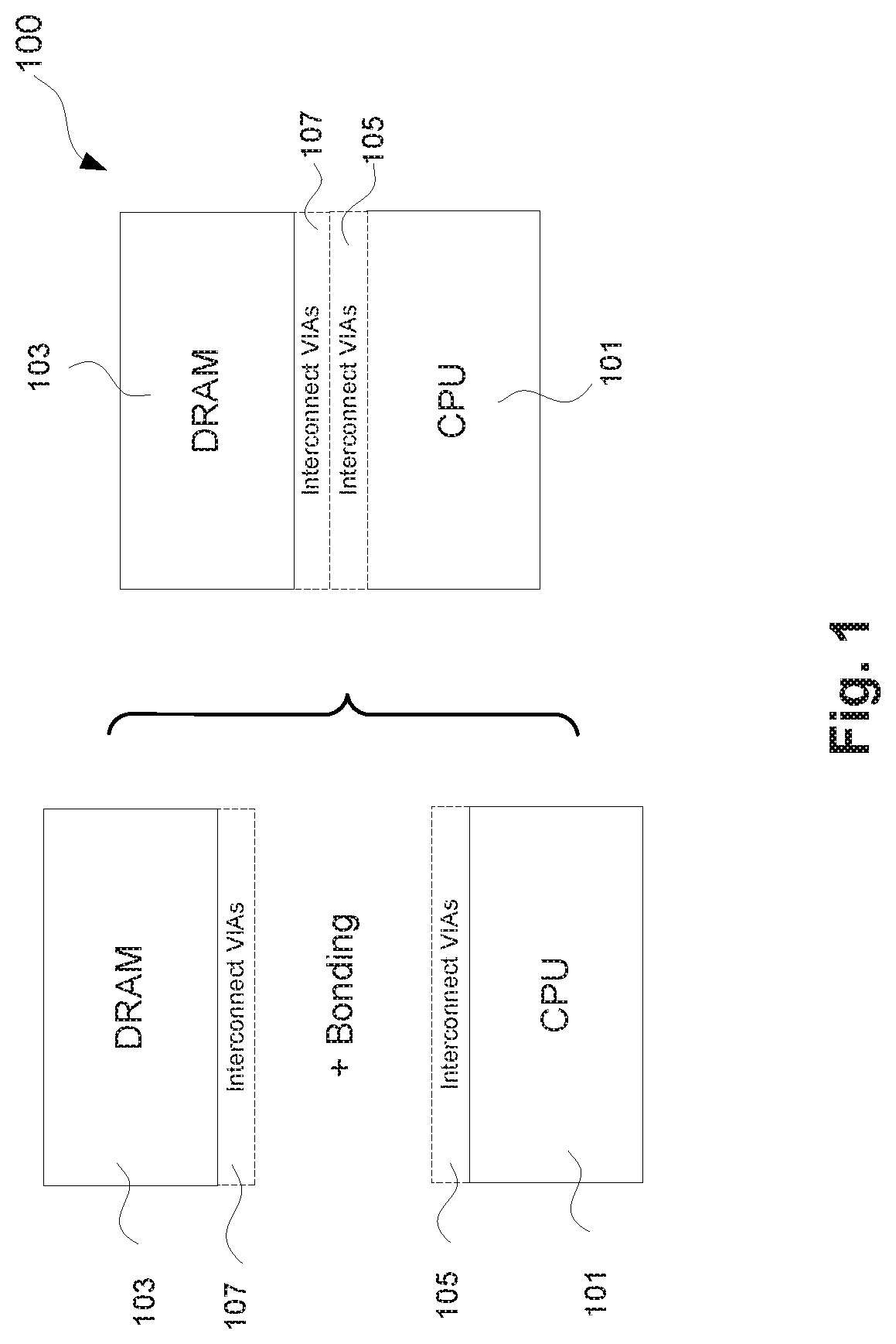
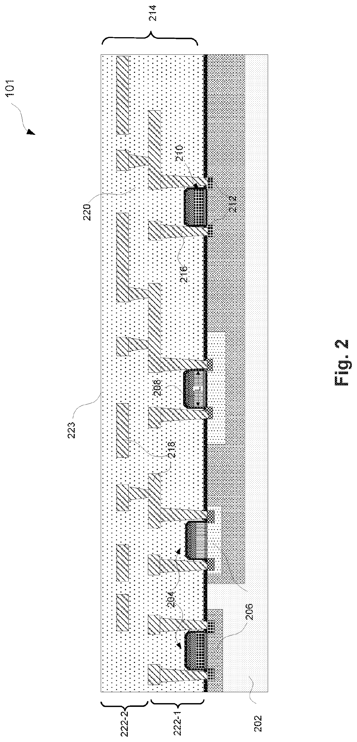
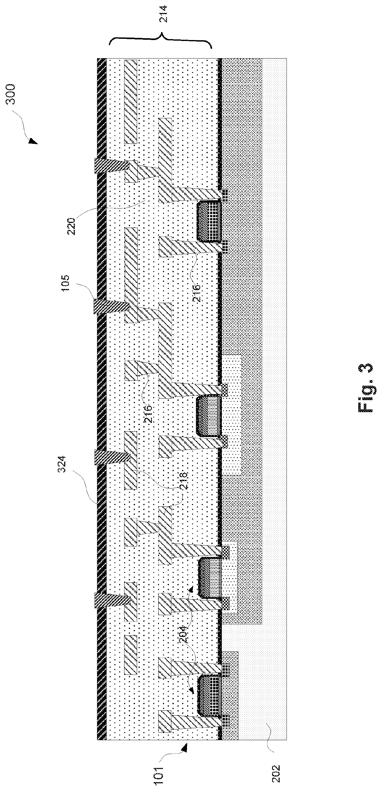
[0063]FIG. 1 illustrates a schematic view of an exemplary 3D IC device 100 according to some embodiments of the present disclosure. 3D IC device 100 can include a microprocessor chip 101 and a memory chip 103. In some embodiments, the microprocessor chip 101 can be any suitable microprocessor, for example, a digital signal processor, a microcontroller, or a central computing unit (CPU) for a computer or a mobile device. In some embodiments, the memory chip 103 can be any suitable volatile or non-volatile memory, for example, a static random-access memory (SRAM), a dynamic random-access memory (DRAM), a phase change memory, a magnetic random-access memory or a flash memory. As an example, the microprocessor chip 101 can be a CPU chip and is also referred to as the CPU chip 101, and the memory chip 103 can be a DRAM chip and is also referred to as the DRAM chip 103. The CPU chip 101 and the...

second embodiment

[0124]An example of the present disclosure will now be described with reference to FIGS. 7 to 15.

[0125]FIG. 7 illustrates a schematic view of an exemplary 3D IC device 700, according to some embodiments of the present disclosure. The 3D IC device 700 can include a microprocessor chip, a first memory chip and a second memory chip. In some embodiments, the microprocessor chip can be any suitable microprocessor, for example, a digital signal processor, a microcontroller, or a central computing unit (CPU) for a computer or a mobile device. In an example, the microprocessor chip can be similar to the microprocessor chip 101 shown in FIGS. 1-3 and is also referred to as the CPU chip 101. In some embodiments, the first memory chip can be any volatile memory, for example, a static random-access memory (SRAM) or a dynamic random-access memory (DRAM). In an example, the first memory chip can be similar to the memory chip 103 shown in FIGS. 1, 4A and 4B and is also referred to as the DRAM chip...


PUM


Abstract

Embodiments of three-dimensional semiconductor devices and fabrication methods are disclosed. The method includes forming a first and a second memory chips and a microprocessor chip. The method also includes bonding a first interconnect layer of the first memory chip with a second interconnect layer of the second memory chip, such that one or more first memory cells of the first memory chip are electrically connected with one or more second memory cells of the second memory chip through interconnect structures of the first and second interconnect layers. The method further includes bonding a third interconnect layer of the microprocessor chip with a substrate of the second memory chip, such that the one or more microprocessor devices of the microprocessor chip are electrically connected with one or more second memory cell of the second memory chip through interconnect structures of the second and third interconnect layers.

Description

CROSS-REFERENCE TO RELATED APPLICATIONS AND INCORPORATION BY REFERENCE[0001]This application claims priority to PCT / CN2019 / 082607 filed on Apr. 15, 2019, which is incorporated herein by reference in its entirety.TECHNICAL FIELD[0002]The present disclosure generally relates to the field of semiconductor technology, and more particularly, to a method for forming a three-dimensional (3D) integrated circuit.BACKGROUND[0003]Planar integrated circuit (IC) devices are scaled to smaller sizes by improving process technology, circuit designs, programming algorithms, and the fabrication process. However, as feature sizes of the logic / analog devices and memory cells approach a lower limit, planar process and fabrication techniques become challenging and costly. As such, density and bandwidth for planar IC devices approach an upper limit. A three-dimensional (3D) IC architecture can address the density and performance limitation in planar IC device.BRIEF SUMMARY[0004]Embodiments of a three-dime...

Claims


Application Information

Patent Timeline
Patent Type & Authority Applications(United States)
IPC IPC(8): H01L25/065H01L25/00H01L23/00
CPCH01L25/0657H01L2224/83896H01L27/11H01L27/108H01L25/50H01L2225/06541H01L27/115H01L24/83H01L2224/83895H01L2224/32146H01L24/32H01L25/18H01L25/0655G11C5/02H01L2224/80895H01L2224/80896H01L2224/09181H01L2224/9202H01L2224/05567H01L2224/03462H01L2224/03464H01L2224/0345H01L2224/03452H01L24/08H01L24/80H01L2224/80357H01L2224/8034H01L2224/05647H01L2224/05655H01L2224/05639H01L2224/05686H01L2224/05644H01L2224/05611H01L2224/05666H01L2224/05624G11C5/025G11C11/005H01L24/05H01L24/29H01L2224/05657H01L2224/05684H01L2224/08145H01L2224/29186H01L2224/32145H01L2924/1437H01L2924/1436H10B12/00H10B12/50H10B10/18H10B10/00H10B69/00H10B43/40H01L2924/00012H01L2224/80001H01L2224/03H01L2924/00014H01L2924/013H01L2924/04953H01L2924/04941H01L27/0688H01L21/823475
Inventor LIU, JUN
Owner YANGTZE MEMORY TECH CO LTD
Why Eureka
Try Eureka