Transistor structure with reduced leakage current and adjustable on/off current
- Summary
- Abstract
- Description
- Claims
- Application Information
AI Technical Summary
Benefits of technology
Problems solved by technology
Method used
Image


Examples
first embodiment
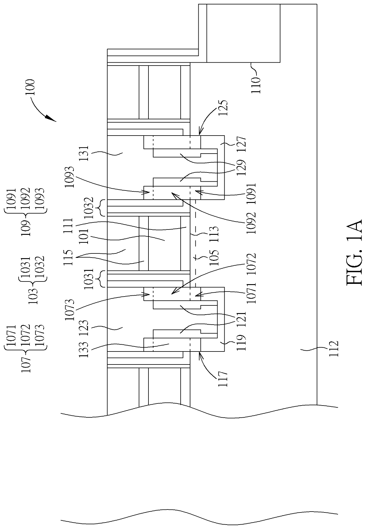
[0040]Please refer to FIG. 1A. FIG. 1A is a diagram illustrating a transistor structure 100 according to the present invention. As shown in FIG. 1A, the transistor 100 includes a gate 101, a spacer 103, a channel region 105, a first conductive region 107, and a second conductive region 109. In addition, a shallow trench isolation (STI) structure 110 is formed next to the transistor structure 100, wherein the STI structure 110 is well-known to those of ordinary skill in the art, so further description thereof is omitted for simplicity. The gate 101 is formed on a dielectric 111, wherein the dielectric 111 is formed on or above a silicon surface 113 of a substrate 112. In addition, a cap structure 115 can be formed on the gate 101. The spacer 103 is formed on or above the silicon surface 113 and includes a first part 1031 and a second part 1032, wherein the first part 1031 covers a left-sidewall of the gate 101, and the second part 1032 covers a right-sidewall of the gate 101. In addi...
second embodiment
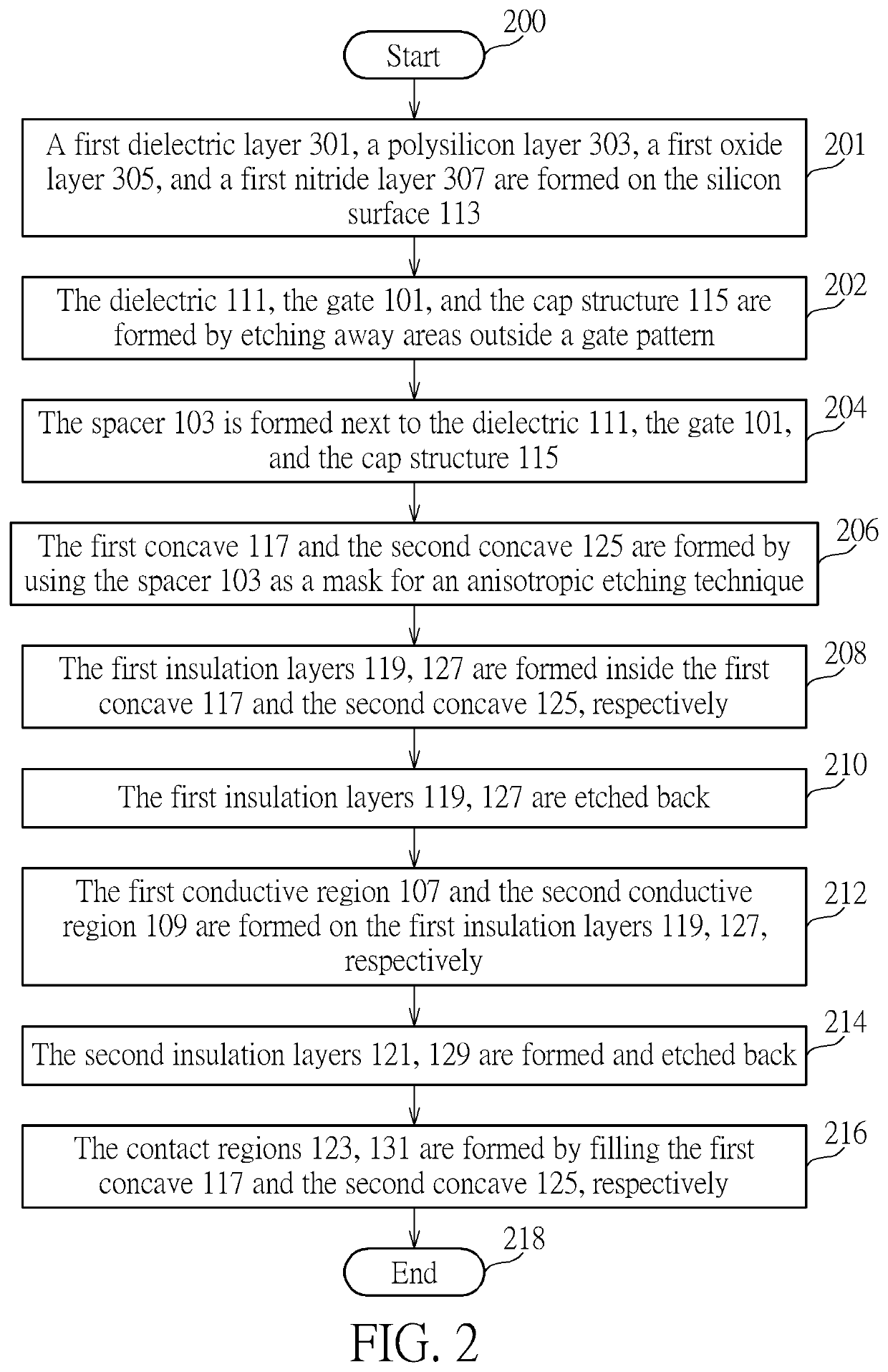
[0050]Please refer to FIGS. 2-11. FIG. 2 is a flowchart illustrating a manufacturing method of the transistor structure 100 according to the present invention. The manufacturing method in FIG. 2 is illustrated using FIGS. 3-11, wherein FIGS. 3-11 also show the neighborhood transistor structure (or neighborhood dummy structure) next to the transistor structure 100, but structures thereof are not labeled in FIGS. 3-11 for simplicity. Detailed steps are as follows:
[0051]Step 200: Start.
[0052]Step 201: A first dielectric layer 301, a polysilicon layer 303, a first oxide layer 305, and a first nitride layer 307 are formed on the silicon surface 113.
[0053]Step 202: The dielectric 111, the gate 101, and the cap structure 115 are formed by etching away areas outside a gate pattern.
[0054]Step 204: The spacer 103 is formed next to the dielectric 111, the gate 101, and the cap structure 115.
[0055]Step 206: The first concave 117 and the second concave 125 are formed by using the spacer 103 as a...
PUM
 Abstract
Description
Claims
Application Information
 - R&D Engineer
- R&D Manager
- IP Professional
- Industry Leading Data Capabilities
- Powerful AI technology
- Patent DNA Extraction
Browse by: Latest US Patents, China's latest patents, Technical Efficacy Thesaurus, Application Domain, Technology Topic.
© 2024 PatSnap. All rights reserved.Legal|Privacy policy|Modern Slavery Act Transparency Statement|Sitemap