Multilayer substrate and antenna module

a technology of antenna modules and substrates, applied in the direction of individual energised antenna arrays, resonant antennas, printed element electric connection formation, etc., can solve the problems of loss relating to column conductors, suppress and reduce the length of pattern conductors constituting feed lines , the effect of reducing the loss of feed lines

Active Publication Date: 2020-10-22
MURATA MFG CO LTD
View PDF0 Cites 5 Cited by
  • Summary
  • Abstract
  • Description
  • Claims
  • Application Information

AI Technical Summary

Benefits of technology

[0030]In such an antenna module, since the RF signal processing circuit is arranged to overlap the region where the patch antenna array is arranged, the length of the pattern conductor constituting the feed line can be reduced, thereby suppressing loss in the feed line. Thus, in particular, such anten...

Problems solved by technology

However, in the configuration of the related art described above, the loss relating to the column conductor is not examined since ensuring connection reliability between the via conductor an...

Method used


Image

  • Multilayer substrate and antenna module
  • Multilayer substrate and antenna module
  • Multilayer substrate and antenna module

Examples


embodiment 1

[0058][1. Overall Configuration of Antenna Module]

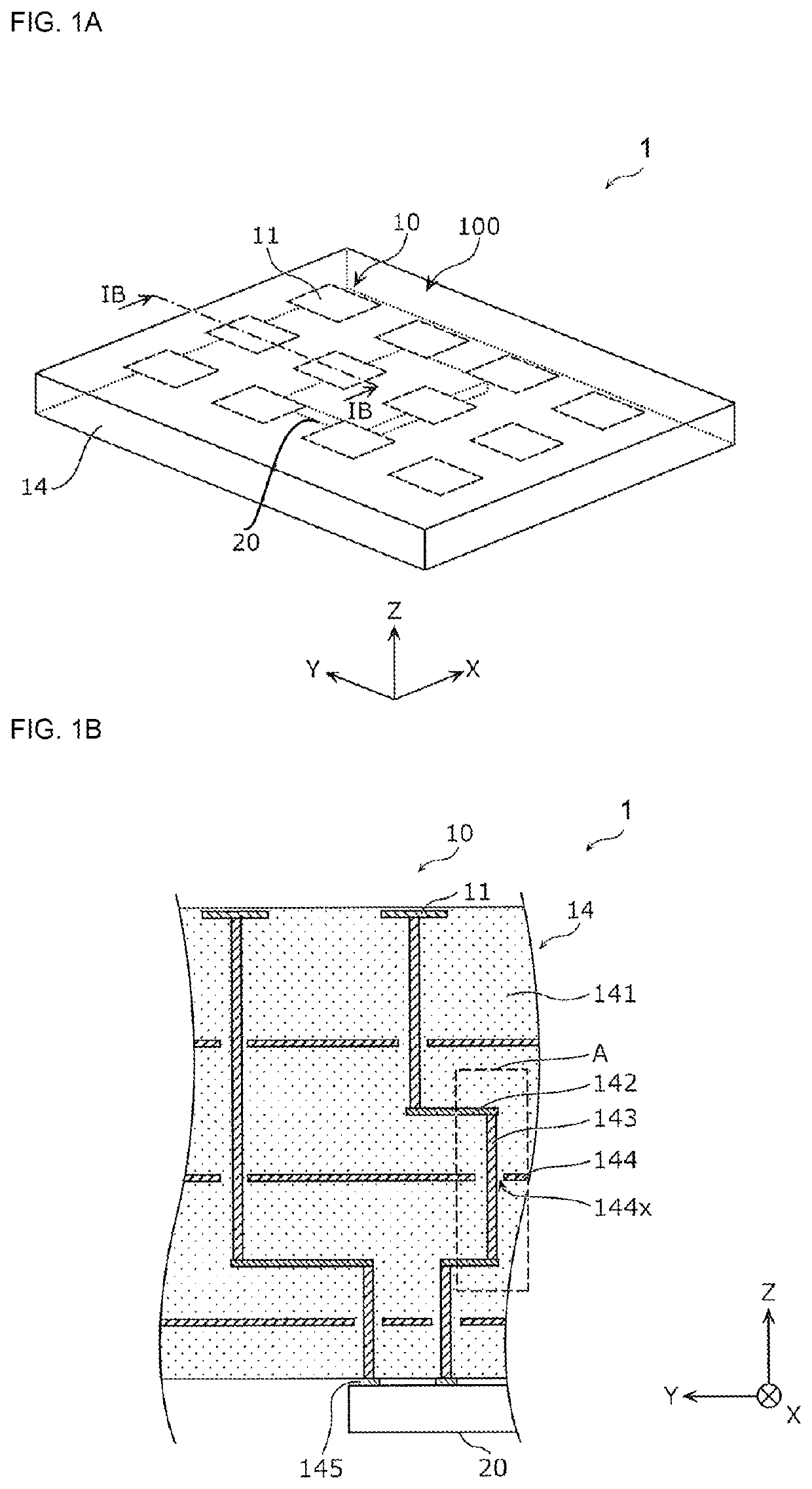
[0059]FIG. 1A is an external perspective view of an antenna module 1 according to an embodiment 1.

[0060]Hereinafter, the thickness direction of the antenna module 1 will be described as a Z axis, directions perpendicular to the Z axis direction and orthogonal to each other are described as an X axis direction and a Y axis direction, respectively. The positive side of the Z axis will be described as a top surface side of the antenna module 1. However, in aspects of actual use, the top surface side of the antenna module 1 is not limited to an upward direction since the thickness direction of the antenna module 1 may not be an up-and-down direction.

[0061]The antenna module 1 illustrated in FIG. 1A includes an antenna array 100 constituted of a plurality of antenna elements 10 and an RFIC 20.

[0062]Each of the plurality of antenna elements 10 is a patch antenna having a radiation conductor 11 composed of a thin film pattern conductor prov...

embodiment 2

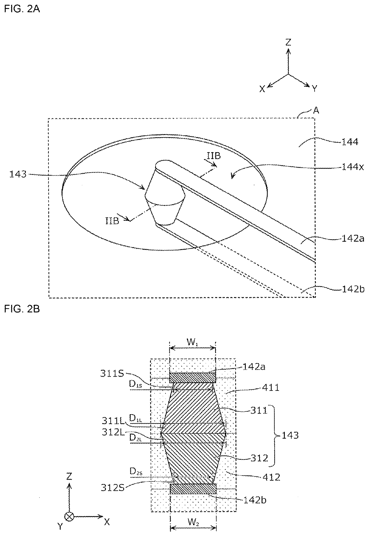
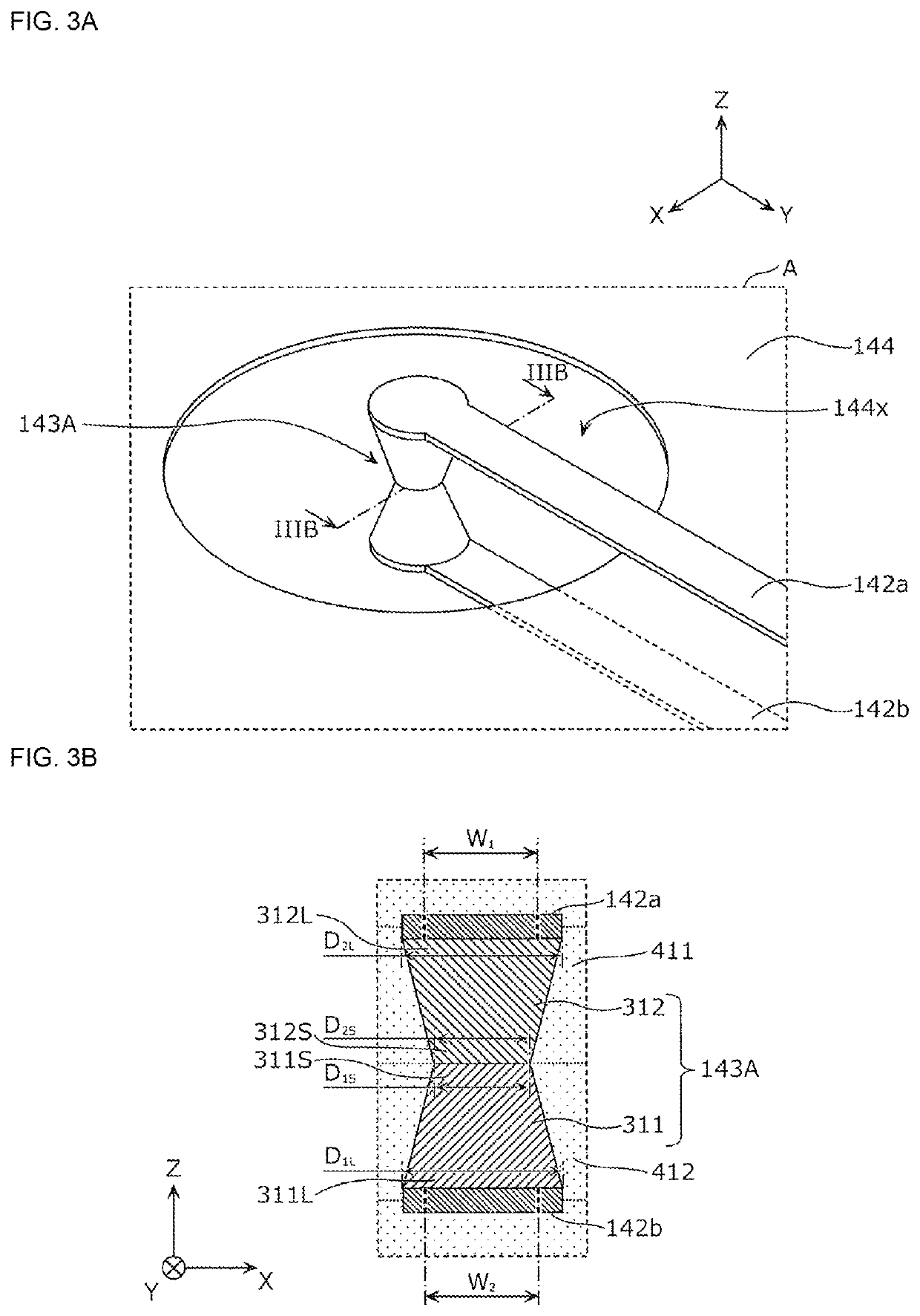
[0154]The aspect of the column conductor formed of the via conductor having the tapered shape described in Embodiment 1 is not limited to the column conductor formed of two via conductors, but can also be applied to the column conductor formed of three or more via conductors. With respect to such column conductor, a description will be given of the multilayer substrate including the column conductor formed of four via conductors stacked in the present embodiment. The number of via conductors constituting the column conductor is equal to the number of insulator layers through which the column conductor extends.

[0155]FIG. 12 is a perspective view of a column conductor 243 and the vicinity thereof according to the present embodiment. Specifically, an enlarged view of the portion corresponding to part A in FIG. 1B is illustrated in FIG. 12. Although two insulator layers are provided between the two wiring conductors 142a and 142b in Embodiment 1, four insulator layers are provided in th...


PUM


Abstract

A multilayer substrate includes a plurality of insulator layers laminated, a column conductor extending through two or more insulator layers among the plurality of insulator layers. The column conductor includes a first via conductor extending through a first insulator layer and a second via conductor extending through a second insulator layer adjacent to the first insulator layer. Each of the first via conductor and the second via conductor has a tapered shape in which a cross section decreases from one end portion to the other end portion in the lamination direction of the plurality of insulator layers. The first via conductor and the second via conductor are directly bonded to each other at large diameter portions that are end portions with a large cross section or small diameter portions that are end portions with a small cross section.

Description

[0001]This is a continuation of International Application No. PCT / JP2018 / 029610 filed on Aug. 7, 2018 which claims priority from Japanese Patent Application No. 2017-165130 filed on Aug. 30, 2017. The contents of these applications are incorporated herein by reference in their entireties.BACKGROUNDTechnical Field[0002]The present disclosure relates to a multilayer substrate and an antenna module.[0003]A multilayer wiring substrate (multilayer substrate), in which a connection pad for connecting to an electronic element is provided on a front surface and a terminal pad for connecting to an external circuit is provided on a back surface, having a configuration with a tapered via conductor is disclosed (for example, refer to Patent Document 1). According to this configuration, the diameter of the via conductor connected to the terminal pad on the back surface is gradually reduced from the back surface side to the front surface side, and on the other hand, the diameter of other via cond...

Claims


Application Information

Patent Timeline
IPC IPC(8): H05K3/46H01Q13/08H01Q21/06H01Q9/04H01Q23/00H01Q1/38H05K1/02H05K1/16H05K3/40
CPCH01Q23/00H01Q1/38H05K1/02H01Q9/0407H05K3/46H01Q13/08H05K3/40H01Q21/06H05K1/16H05K1/165H05K2201/10098H05K1/115H05K2201/09827H05K2201/09563H05K3/429H05K2201/096H05K2201/09609H05K2201/09618H05K1/0225H05K2201/09845H01Q21/065H01Q1/2283H01P5/02
Inventor ARIUMI, SANEAKI
Owner MURATA MFG CO LTD
Why Eureka
Try Eureka