Monolithic solar cell and method of manufacturing the same

a solar cell and monolithic technology, applied in the field can solve the problems of high manufacturing cost, limited photoelectric conversion efficiency of single-junction solar cells, and extremely limited field use of v compound-based tandem solar cells, so as to improve photoelectric conversion efficiency, improve charge transfer and recombination characteristics, and prevent optical loss at the interface during the manufacture of monolithic solar cells

Active Publication Date: 2020-10-29
KOREA INST OF SCI & TECH
View PDF0 Cites 1 Cited by
  • Summary
  • Abstract
  • Description
  • Claims
  • Application Information

AI Technical Summary

Benefits of technology

[0025]In accordance with the present invention, an interfacial layer is provided between two cells constituting a monolithic solar cell, thereby improving charge transfer and recombination characteristics between the two cells. Accordingly, a monolithic solar cell having significantly improved photoelectric conversion efficiency can be provided.
[0026]In addition, in accordance with the present invention, the interfacial layer, which is inserted into an interface between two cells constituting the monolithic solar cell and is constituted of an organic material, can be partially or completely pyrolyzed and thus lost during a heat treatment process. Accordingly, optical loss occurring at the interface during manufacture of the monolithic solar cell can be prevented, and electrical loss at the interface can be minimized, which allows the manufacture of a highly efficient monolithic solar cell.
[0027]Further, a method of manufacturing a monolithic solar cell according to the present invention can overcome the efficiency limit of the silicon solar cell without greatly increasing the manufacturing costs of the silicon solar cell because a perovskite cell constituting the monolithic solar cell is manufactured based on a simple solution process.

Problems solved by technology

However, the theoretical photoelectric conversion efficiency (hereinafter referred to as efficiency) of a single-junction solar cell is limited to a maximum of about 33% (Shockley-Queisser limit) because surplus energy of electrons-holes generated due to the absorption of photons having energy larger than a band gap by the semiconductor is inevitably lost as heat (thermalization loss), whereas photons having energy lower than the band gap pass through the semiconductor without being absorbed thereby.
However, group III-V compound-based tandem solar cells are used in extremely limited fields such as a spacecraft due to the complexity of the epitaxial deposition technique used in manufacture thereof and high manufacturing costs due to the use of expensive equipment.
On the other hand, with regard to amorphous / polycrystalline silicon tandem solar cells having relatively high price competitiveness, LG Electronics reported a triple junction solar cell with an efficiency of 13.4% in 2012, but the efficiency is still too low to allow commercialization.
Thus, attempts to apply a perovskite solar cell to a tandem architecture are under intense competition around the world.
If the properties of the thin transparent electrode are different from those of a transparent electrode substrate used to manufacture a single-junction perovskite solar cell, charge transfer or recombination between the two subcells may not be smoothly performed.

Method used


Image

  • Monolithic solar cell and method of manufacturing the same
  • Monolithic solar cell and method of manufacturing the same
  • Monolithic solar cell and method of manufacturing the same

Examples


experimental example

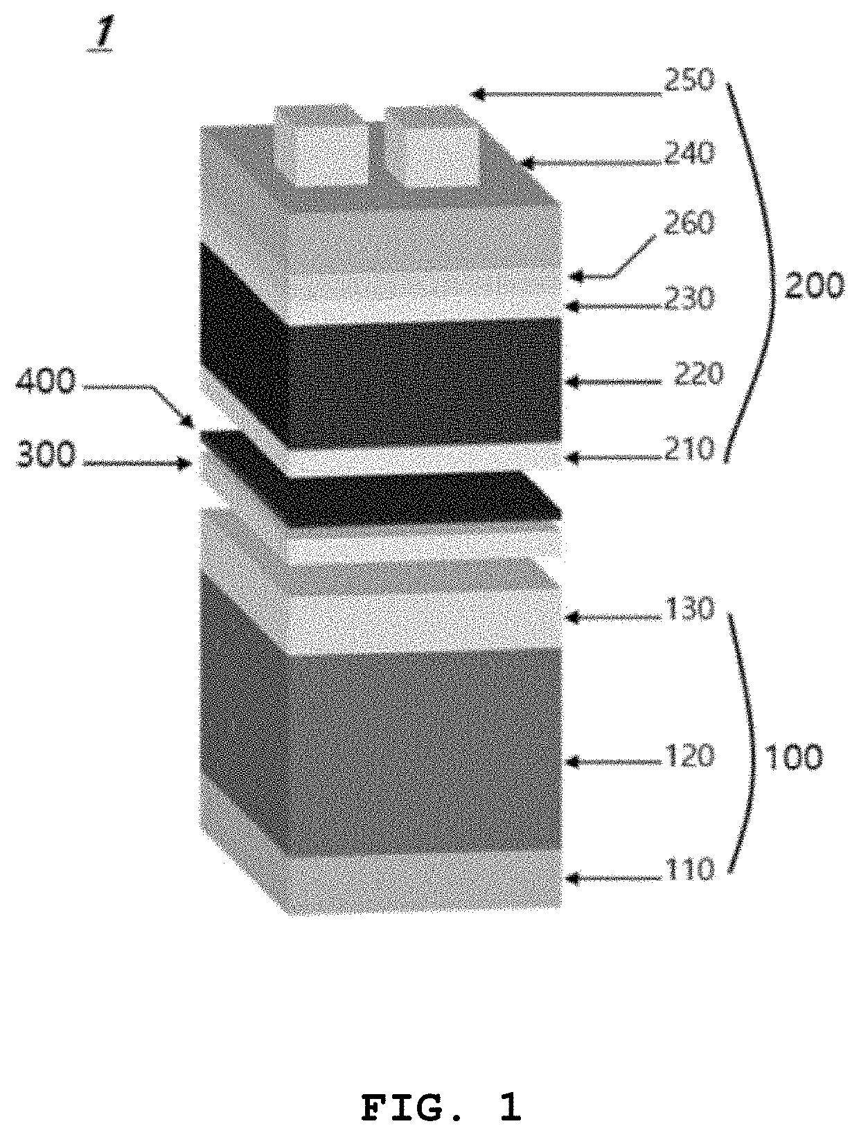
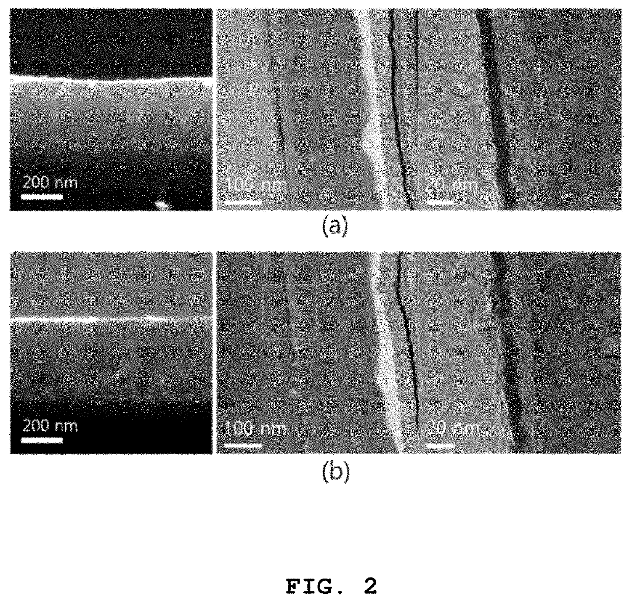
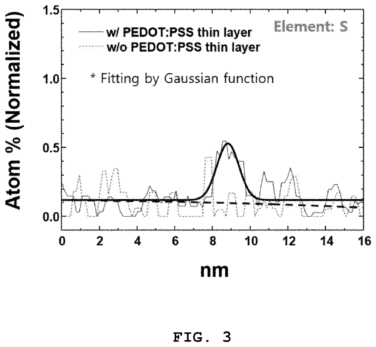
[0057]To manufacture monolithic solar cells including an interfacial layer (organic sacrificial layer) according to various embodiments of the present invention, a first solar cell, which was a silicon solar cell type, was prepared, an ITO-type tunnel junction layer was formed on an n-type emitter of the first solar cell, a PEDOT:PSS interfacial layer (or organic sacrificial layer) was formed on the ITO-type tunnel junction layer, and a second solar cell, which was a perovskite solar cell type, was laminated on the PEDOT:PSS interfacial layer.

[0058]Here, the PEDOT:PSS interfacial layer was manufactured by diluting PEDOT:PSS (Clevios™ P VP AI 4083), manufactured by Heraeus, with methanol, and then forming a PEDOT:PSS thin-film by spin-coating, followed by heat-treatment at 150° C. for 20 minutes.

[0059]A second solar cell, which is a perovskite solar cell type, was manufactured by sequentially laminating a p-type hole-selective film, a perovskite, an n-type electron-selective film, a ...


PUM

PropertyMeasurementUnit
band gapaaaaaaaaaa
band gapaaaaaaaaaa
transparentaaaaaaaaaa

Abstract

Disclosed are a monolithic solar cell and a method of manufacturing the same. More particularly, the present invention provides a monolithic solar cell including a first solar cell formed by sequentially stacking an electrode, a silicon substrate, and an n-type emitter layer; a junction layer formed on the an n-type emitter layer; an interfacial layer formed on the junction layer; and a second solar cell including a perovskite layer and integrated onto the interfacial layer. The interfacial layer according to the present invention may be pyrolyzed and thus partially or completely lost during a monolithic solar cell manufacturing process. In addition, by providing an interfacial layer between the two cells constituting a monolithic solar cell according to the present invention, charge transfer and recombination characteristics between the two cells can be improved and thus a monolithic solar cell having significantly improved photoelectric conversion efficiency can be provided.

Description

TECHNICAL FIELD[0001]The present invention relates to a technology of tandem integration of perovskite solar cell onto a silicon solar cell, and more particularly, to a monolithic solar cell, on which a silicon solar cell and a perovskite solar cell are stacked in series, including an interfacial layer (organic sacrificial layer) capable of improving charge transfer or recombination at an interface between the two cells and a method of manufacturing the monolithic solar cell.BACKGROUND ART[0002]As the depletion of fossil reserves and the global warming phenomenon become more and more widespread, interest in solar energy, which is an environmentally friendly and infinite energy source, is increasing. Photovoltaic energy can be utilized as a distributed power source in areas where external power supply is difficult as well as large-scale power generation because it has few geographical constraints and is safe in terms of utilization. In recent years, demand for photovoltaic energy tec...

Claims


Application Information

Patent Timeline
Patent Type & Authority Applications(United States)
IPC IPC(8): H01L27/30H01L27/28H01G9/20
CPCH01L27/302H01G9/2059H01L27/286Y02P70/50Y02E10/542Y02E10/549H01L31/043H10K30/57H10K85/1135H10K30/10H10K85/50H01L31/022475H01L31/022483H01L31/032H01L31/046H01L31/0504H01L31/0725H01L31/18H01L31/0687H10K19/20H10K30/151H10K30/152
Inventor LEE, DOH KWONJANG, YOON HEEKIM, IN HOYUN, HEE SUNJEONG, JEUNG HYUN
Owner KOREA INST OF SCI & TECH
Why Eureka
Try Eureka