Assembly structure and electronic device having the same

a technology of assembly structure and electronic device, which is applied in the association of printed circuit non-printed electric components, instruments, and modifications by conduction heat transfer, etc., can solve the problems of increasing power consumption of chips, increasing space occupancy and power consumption, and increasing losses on a current path from power source modules to chips, so as to shorten the current path

Active Publication Date: 2020-12-17
DELTA ELECTRONICS INC
View PDF0 Cites 1 Cited by
  • Summary
  • Abstract
  • Description
  • Claims
  • Application Information

AI Technical Summary

Benefits of technology

[0012]The present disclosure assembles a power converting module with a circuit board and a chip in a stacking manner, which may shorten a current path between the power converting module and the chip.

Problems solved by technology

With increase of processing capacity per volume unit of a server, the amount and integration level of the processing chips are also increasing, resulting in increase of space occupancy and power consumption.
Along with increase of computing speeds of chips, power consumption of the chips increases.
Although supply voltages of the chips trend to be reduced, supply currents are still increased greatly due to increase of amount of transistors, which causes that losses on a current path from the power source modules to the chips increase greatly and whole efficiency of systems are reduced.
Such structural members occupy much space around the chip 12, so that the power supply module 13 cannot be close to the processor chip 12, which results in a long current path and more losses.
In some applications, the losses may even reach 2% of total power consumption of the chip.
Heights of the power supply modules are hard to be lower than the body heights of the chips.
Limited by sizes of the heat sinks, the power supply modules cannot be placed in positions close to the chips, which results in long current paths and more losses.

Method used


Image

  • Assembly structure and electronic device having the same
  • Assembly structure and electronic device having the same
  • Assembly structure and electronic device having the same

Examples


Embodiment Construction

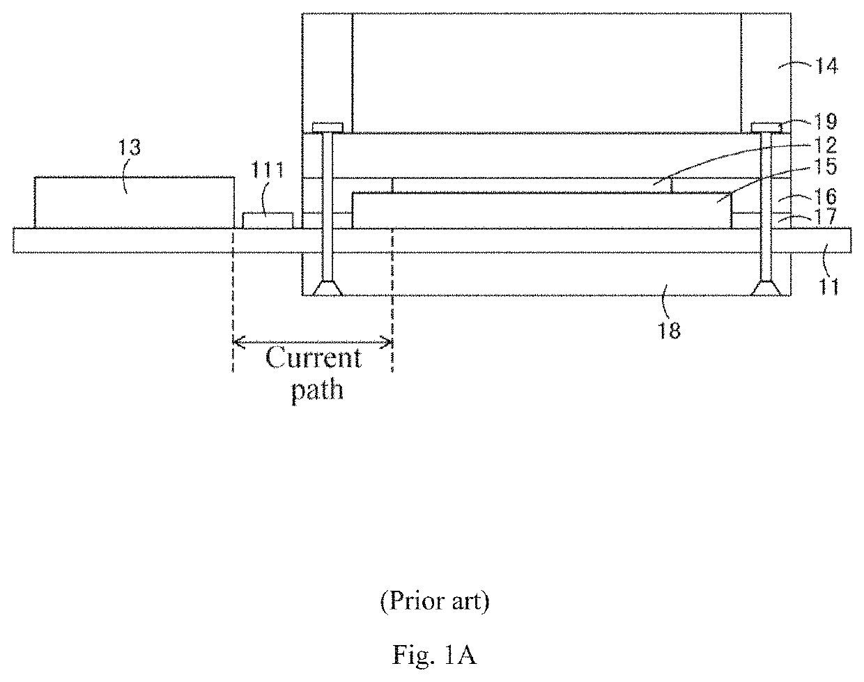
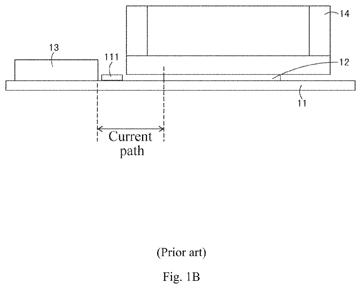
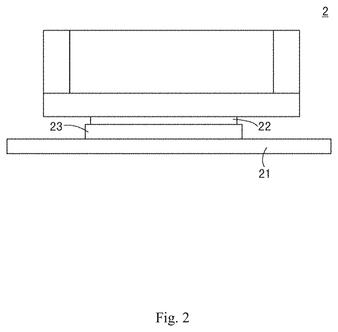
[0038]FIG. 2 is a schematic diagram of an assembly structure for providing power for a chip of an embodiment of the present disclosure. The assembly structure 2 for providing power for a chip includes a circuit board 21, which provides a first electrical energy; a chip 22, which may be a CPU, a GPU or a memory and the like; and a power converting module 23, which is electrically connected to the circuit board 21 and the chip 22, converts the first electrical energy to a second electrical energy, and supplies the second electrical energy to the chip 22. Wherein the power converting module 23 may be located between the chip 22 and the circuit board 21 and they are mutually stacked to form the assembly structure 2. However, the present disclosure is not limited to this. An upper surface of the power converting module 23 and a lower surface of the chip 22 may be contacted and electrically connected. A lower surface of the power converting module 23 and an upper surface of the circuit bo...


PUM


Abstract

The present disclosure provides an assembly structure for providing power for a chip and an electronic device using the same. The assembly structure includes: a circuit board, configured to provide a first electrical energy; a chip; a power converting module, configured to electrically connect the circuit board and the chip, convert the first electrical energy to a second electrical energy, and supply the second electrical energy to the chip, wherein the chip, the circuit board and the power converting module are stacked; and a connection component, configured to electrically connect the circuit board and the power converting module. The present disclosure assembles a power converting module with a circuit board and a chip in a stacking manner, which may shorten a current path between the power converting module and the chip, reduce current transmission losses, improve efficiency of a system, reduce space occupancy and save system resource.

Description

CROSS-REFERENCE TO RELATED APPLICATIONS[0001]This application is a Continuation of U.S. application Ser. No. 15 / 164,214, filed on May 25, 2016, which is based upon and claims priority to Chinese Patent Application No. 201510362342.2, filed Jun. 26, 2015, the entire contents of which are incorporated herein by reference.TECHNICAL FIELD[0002]The present disclosure relates to an assembly structure and an electronic device, and more particularly, to an assembly structure for providing power for a chip and an electronic device having the assembly structure.BACKGROUND[0003]With growth of demand for intelligent life of people, demand for data processing is also growing. Throughout the world, power consumption spent on data processing has reached hundreds of billions of or even trillions of kilowatts-hours each year on average, and a large data center may occupy an area up to tens of thousands of square meters. Accordingly, high efficiency and high power density are key pointers of healthy ...

Claims


Application Information

Patent Timeline
Patent Type & Authority Applications(United States)
IPC IPC(8): H05K7/02H05K7/10H05K1/14H05K1/02G06F1/20G06F1/18H05K1/18H05K7/20
CPCH05K2201/1053H05K2201/10515H05K2201/10545H05K1/141H05K1/0262H05K1/0218H05K7/02H05K2201/10325H05K7/10G06F1/20H05K2201/10189G06F1/188H05K3/368H01L25/165H05K7/2039H05K1/182H05K1/181Y02D10/00H01L23/36H01L25/105H01L2225/1058H01L23/4006H01L23/552
Inventor YE, HAOYIZENG, JIANHONGZHANG, YUHU, PEIQINGZHOU, ZIYING
Owner DELTA ELECTRONICS INC
Why Eureka
Try Eureka