
Three-dimensional memory device and manufacturing method thereof

a three-dimensional memory and manufacturing method technology, applied in the direction of semiconductor devices, electrical appliances, basic electric elements, etc., can solve the problems of three-dimensional nand flash memory, and achieve the effects of improving device performance, widening process windows, and increasing the total aspect ratio of vertical channel pillars

Active Publication Date: 2021-01-21
MACRONIX INT CO LTD
View PDF1 Cites 4 Cited by
  • Summary
  • Abstract
  • Description
  • Claims
  • Application Information

AI Technical Summary

Benefits of technology

The present invention provides a three-dimensional memory device and a manufacturing method with improved device performance. The invention increases the total aspect ratio of vertical channel pillars and adds an etching stop layer between adjacent vertical channel pillars to widen the process window of misalignment. This prevents damage to the underlying first vertical channel pillar caused by misalignment of the second opening and improves device performance. Additionally, the etching stop layer can act as a floating node or an operation node based on electrical requirements, increasing design flexibility of the product.

Problems solved by technology

However, there are still some challenges associated with the three-dimensional NAND flash memory.

Method used


Image

  • Three-dimensional memory device and manufacturing method thereof
  • Three-dimensional memory device and manufacturing method thereof
  • Three-dimensional memory device and manufacturing method thereof

Examples


Embodiment Construction

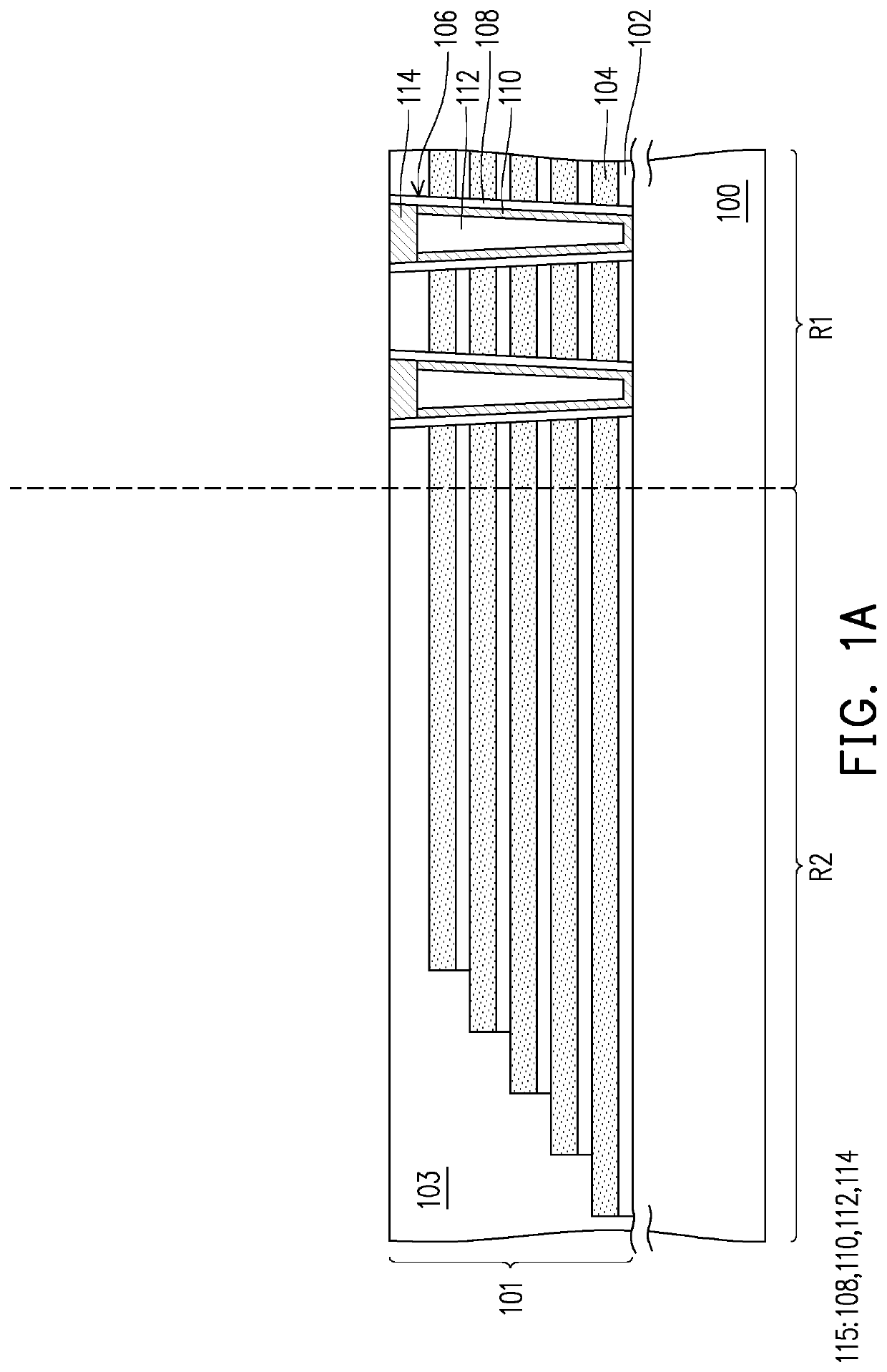
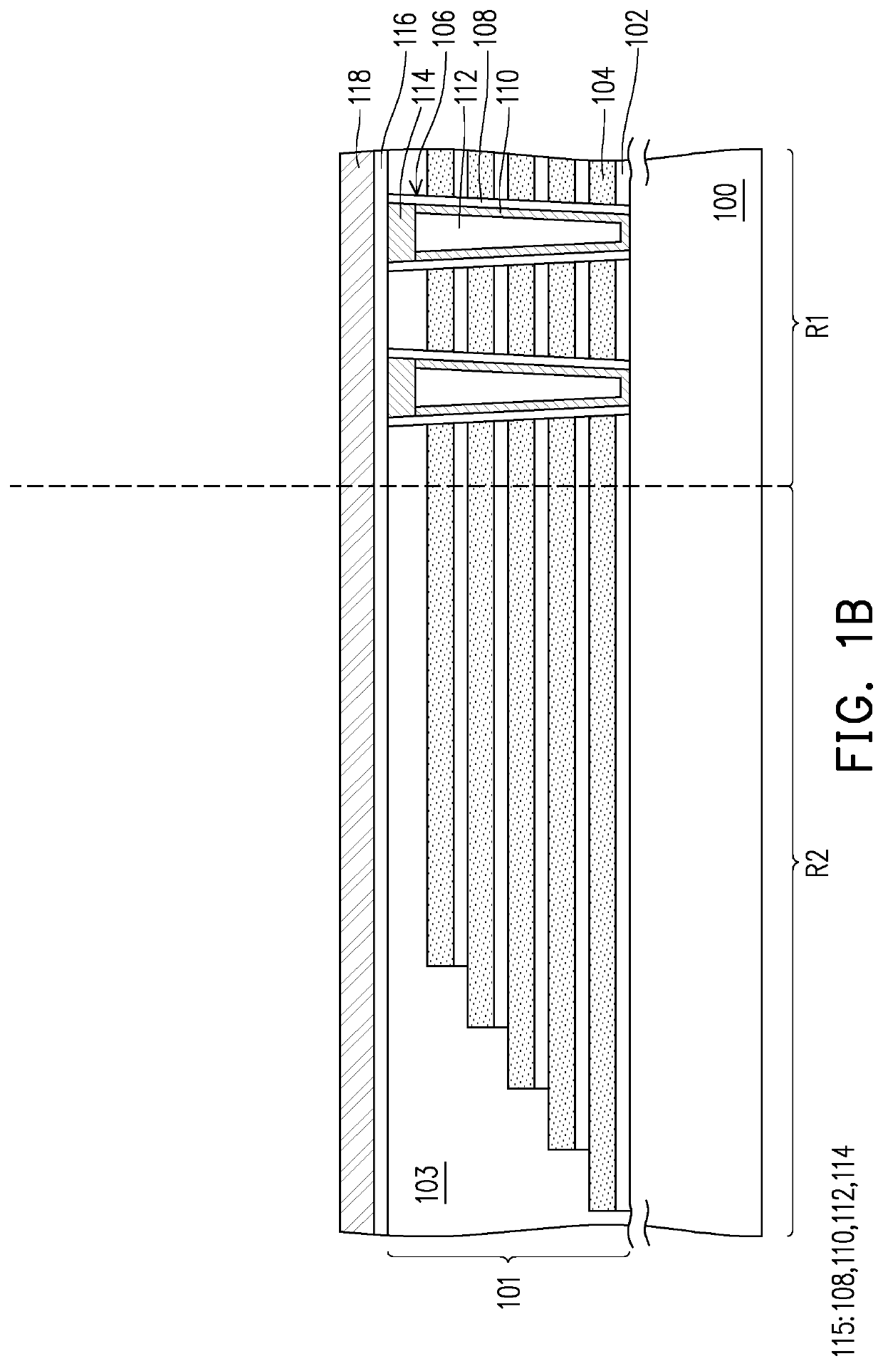
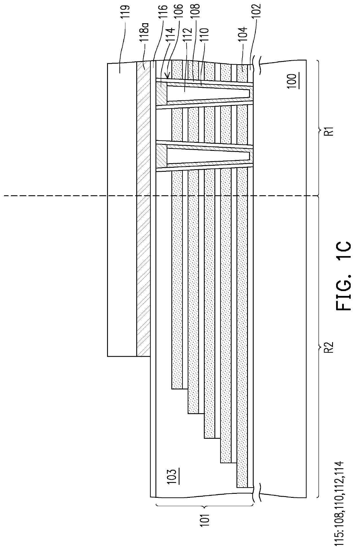
[0033]FIG. 1A to FIG. 1I are schematic cross-sectional views of a method of forming a three-dimensional memory device according to an embodiment of the present invention. FIG. 2 is a schematic cross-sectional view of a three-dimensional memory device according to another embodiment of the present invention. FIG. 3 is a schematic cross-sectional view of a three-dimensional memory device according to yet another embodiment of the present invention.

[0034]Referring to FIG. 1A, a substrate 100 is provided. The substrate 100 can be a semiconductor substrate, such as a silicon-containing substrate. In an embodiment, upon the design requirement, the substrate 100 has a doped region formed therein. In an embodiment, the substrate 100 has a cell region R1 and a periphery region R2.

[0035]Thereafter, a first stacked structure 101 is formed on the substrate 100. In an embodiment, the first stacked structure 101 is disposed on the cell region R1 and the periphery region R2. In an embodiment, the ...


PUM


Abstract

Provided is a three-dimensional memory device including a substrate, first and second stacked structures and an etching stop layer. The substrate has a cell region and a periphery region. The first stacked structure is disposed on the cell region and the periphery region, and has a first vertical channel pillar on the cell region that penetrates through the first stacked structure. The second stacked structure is located on the first stacked structure, is disposed on the cell region and the periphery region, and has a second vertical channel pillar on the cell region that penetrates through the second stacked structure. The second vertical channel pillar is electrically connected to the first vertical channel pillar. The etching stop layer is located between the first and second stacked structures, is disposed on the cell region and extends onto the periphery region, and surrounds the lower portion of the second vertical channel pillar.

Description

BACKGROUNDTechnical Field[0001]The present invention is related to a semiconductor device and a manufacturing method thereof, and more generally to a three-dimensional memory device and a manufacturing method thereof.Description of Related Art[0002]Since a non-volatile memory (e.g., flash memory) has the advantage that stored data does not disappear at power-off, it becomes a widely used memory device for a personal computer or other electronics equipment.[0003]Currently, the flash memory array commonly used in the industry includes a NOR flash memory and a NAND flash memory. Since the NAND flash memory has a structure in which memory cells are connected together in series, degree of integration and area utilization thereof are better than those of the NOR flash memory. Thus, the NAND flash memory has been widely used in a variety of electronic products. Besides, to further enhance the degree of integration of the memory device, a three-dimensional NAND flash memory is developed. Ho...

Claims


Application Information

Patent Timeline
IPC IPC(8): H01L27/11582H01L21/04H01L21/306H01L27/02
CPCH01L27/11582H01L27/0207H01L21/30604H01L21/042H10B43/35H10B43/27H10B41/50H10B43/50H10B41/27
Inventor YANG, CHIH-KAIHAN, TZUNG-TING
Owner MACRONIX INT CO LTD
Learn More