Eureka AIR delivers breakthrough ideas for toughest innovation challenges, trusted by R&D personnel around the world.

Heat utilizing device

a technology of heat utilizing device and heat dissipation device, which is applied in the direction of heat measurement, optical radiation measurement, instruments, etc., can solve the problems of limited heat dissipation from the thermistor through the atmosphere, limited heat dissipation in the support member, and limited heat dissipation in the wiring layer, so as to improve the temperature increase efficiency of the thermistor, and limit the effect of radiation hea

Active Publication Date: 2021-01-28
TDK CORPARATION
View PDF0 Cites 0 Cited by
  • Summary
  • Abstract
  • Description
  • Claims
  • Application Information

AI Technical Summary

Benefits of technology

The present invention aims to provide a heat utilizing device where the thermal resistance of the wiring layer is increased while limiting the increase in electric resistance of the wiring layer. This is achieved by using a support member made of an insulating material with high physical strength, but the wiring layer is made of a conductive material. This configuration helps to reduce heat conduction in the support member and minimize measurement error of the thermistor due to an increase in heat generated by the wiring layer.

Problems solved by technology

Thus, the heat dissipation from the thermistor through the atmosphere, as well as the heat dissipation from the thermistor to the housing through heat conduction, are limited.
As a result, heat conduction in the support member is limited, but heat conduction in the wiring layer may reach a level that is not negligible.
If the wiring layer is made of a material having low electric conductivity, then heat conduction can be limited, but an increase in electric resistance leads to an increase in power consumption.
In addition, due to an increase of heat that is generated by the wiring layer, measurement error of the thermistor may be increased.

Method used


Image

  • Heat utilizing device
  • Heat utilizing device
  • Heat utilizing device

Examples


first embodiment

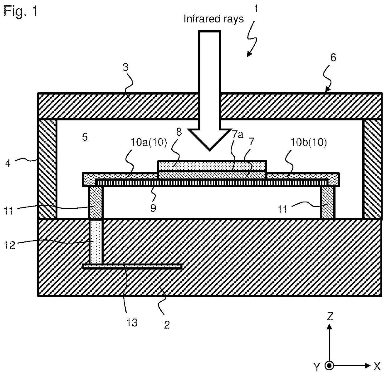
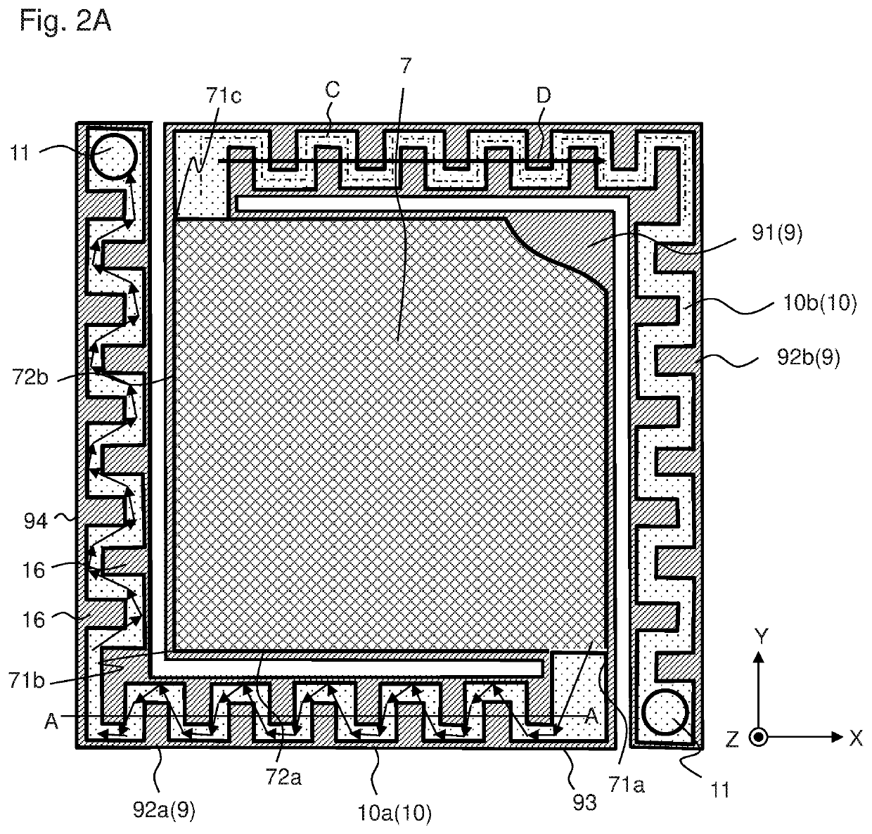
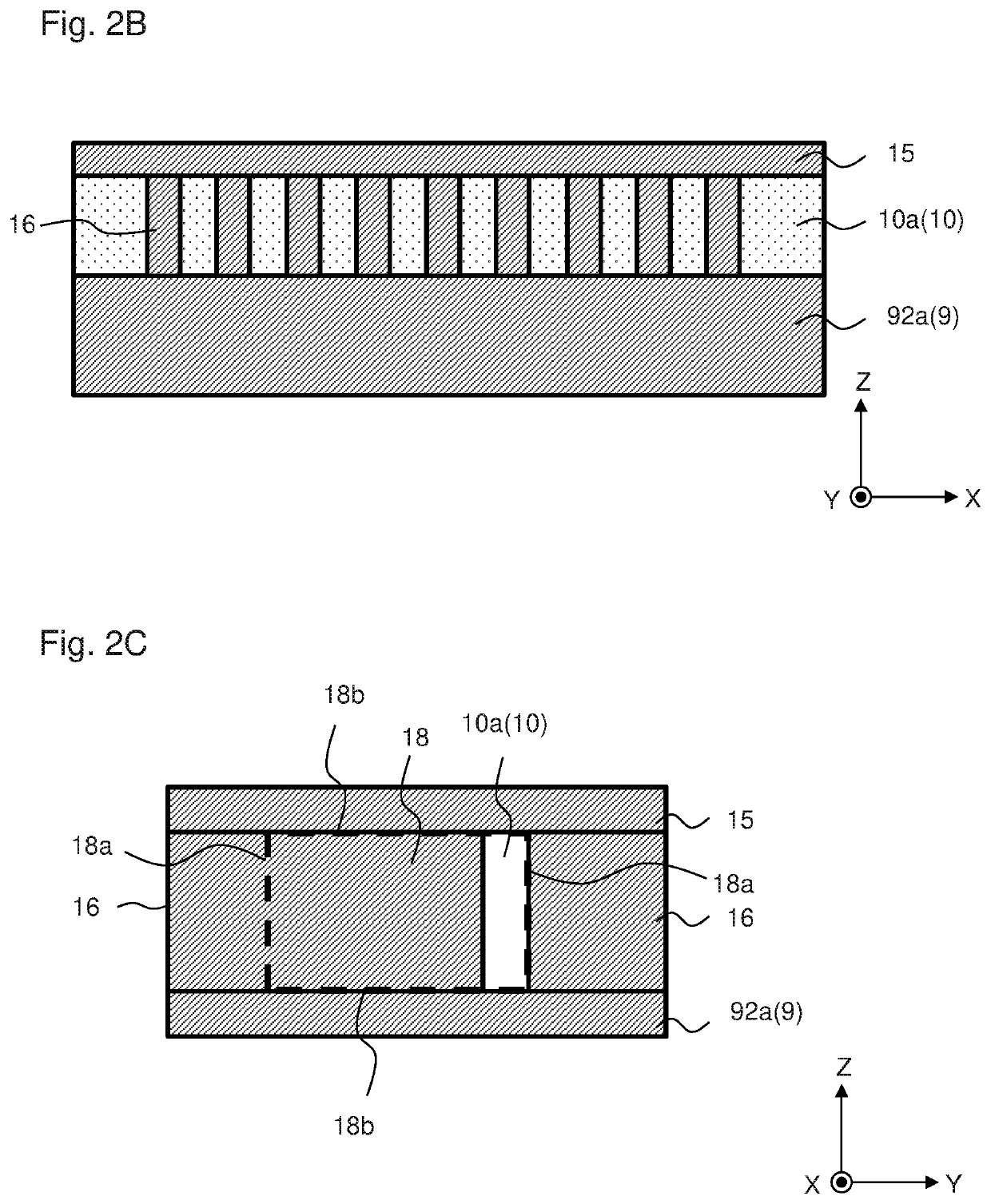
[0056]FIG. 1 is a schematic side view of infrared sensor 1 of the first embodiment of the present invention, FIG. 2A is a schematic plan view in the vicinity of the thermistor film, FIG. 2B is a sectional view of wiring layer 10 taken along line A-A in FIG. 2A, and FIG. 2C is a sectional view of wiring layer 10, as viewed in the X direction. Thermistor film 7 is partially omitted in FIG. 2A in order to show central portion 91 of support layer 9.

[0057]Infrared sensor 1 has first substrate 2, second substrate 3 that faces first substrate 2, as well as side walls 4 that connect first substrate 2 and second substrate 3. Second substrate 3 is a window substrate into which infrared rays enter. First substrate 2, second substrate 3 and side walls 4 form tightly closed inner space 5. Thermistor film 7 is housed in inner space 5. Inner space 5 is at a negative pressure or forms a vacuum.

[0058]That is, first substrate 2, second substrate 3 and side walls 4 form tightly closed vacuum housing 6...

second embodiment

[0071]FIG. 5A is a schematic plan view in the vicinity of thermistor film 7 of the infrared sensor of the second embodiment, and FIG. 5B shows a sectional view of wiring layer 20 taken along line A-A in FIG. 5. Here, the difference from the first embodiment will be mainly described. Configurations and effects that are not explained are the same as those of the first embodiment.

[0072]In the present embodiment, wiring layer 20 is separated or divided in the thickness direction (the Z direction) by separating layer 17. First wiring layer 21 is formed on support layer 9 (first arm portion 92a and second arm portion 92b), separating layer 17 is formed on first wiring layer 21, second wiring layer 22 is formed on separating layer 17, and second wiring layer 22 is covered with first insulating layer 15. Separating layer 17 is made of one or more materials selected from the group consisting of AlN, AlOx, diamond-like carbon, SiNx, SiOx, TaOx, and TiO2. Separating layer 17 may be made of the...

third embodiment

[0075]FIG. 6A shows a schematic plan view in the vicinity of thermistor film 7 of the infrared sensor of the third embodiment, FIG. 6B shows an enlarged view of portion A in FIG. 6, and FIG. 6C shows a sectional view of portion A, as viewed in the X direction. Here, the difference from the first embodiment will be mainly described. Configurations and effects that are not explained are the same as those of the first embodiment.

[0076]In the present embodiment, wiring layer 30 is separated or divided in the width direction by separating layers 31. More specifically, wiring layer 30 is separated or divided in the Y direction by separating layers 31 in first portion 93 of first arm portion 92a and is separated or divided in the X direction by separating layers 31 in second portion 94. First to fourth wiring layers 30a to 30d that extend in parallel with each other are formed on support layer 9 (first arm portion 92a), with first separating layer 31a being provided between first wiring la...


PUM

PropertyMeasurementUnit
wave lengthaaaaaaaaaa
electric resistanceaaaaaaaaaa
temperatureaaaaaaaaaa

Abstract

A heat utilizing device is provided in which the thermal resistance of the wiring layer is increased while an increase in electric resistance of the wiring layer is limited. Heat utilizing device has thermistor whose electric resistance changes depending on temperature; and wiring layer that is connected to thermistor. A mean free path of phonons in wiring layer is smaller than a mean free path of phonons in an infinite medium that consists of a material of wiring layer.

Description

FIELD OF THE INVENTION[0001]The present invention relates to a heat utilizing device, particularly to a heat utilizing device having a thermistor whose electric resistance changes depending on temperatureBACKGROUND OF THE INVENTION[0002]The electrical resistance of a thermistor that is used as a thermal element in various types of temperature sensors changes depending on temperature. Therefore, the temperature around the thermistor can be detected by detecting a change in electric resistance of the thermistor. When a change in the temperature of the thermistor is caused by radiation heat, the temperature of an object that emits the radiation heat can be detected based on Stefan-Boltzmann law.[0003]An effective way to improve the sensitivity of a thermistor, is to improve the thermal absorptivity of the thermistor. JP 5866881 and JP 60302732 disclose an infrared temperature sensor in which a lead that is connected to a thermal element for detecting infrared rays is formed in a meande...

Claims


Application Information

Patent Timeline
Patent Type & Authority Applications(United States)
IPC IPC(8): G01K7/22H01C7/06
CPCG01K7/22H01C7/06G01J1/02H01C7/008H01C1/012H01C1/08
Inventor HARA, SHINJIOHTA, NAOKIAOKI, SUSUMUKOMURA, EIJIKAIZU, AKIMASA
Owner TDK CORPARATION
Why Eureka
Eureka Blog
Learn More