Engineered current-density profile diode laser

a current density and profile technology, applied in semiconductor lasers, laser details, laser optical resonator construction, etc., can solve the problems of reducing power conversion efficiency, unable to scale brightness and power through cavity length scaling, and long cavity length diode lasers suffering from large asymmetry in photon density, carrier density, gain and recombination lifetime along the length of the cavity, etc., to achieve higher reliable output power, reduce current density, and improve the effect of electrical to optical conversion efficiency

Active Publication Date: 2021-02-25
LAWRENCE LIVERMORE NAT SECURITY LLC
View PDF4 Cites 0 Cited by
  • Summary
  • Abstract
  • Description
  • Claims
  • Application Information

AI Technical Summary

Benefits of technology

[0006]Several techniques for controlling the longitudinal current density profile in a high-power diode laser are described. For example, patterning of the epi-side dielectric with apertures or producing apertures through proton implantation allows control of the current density profile at the quantum wells through the adjustment of the spacing between these features due to lateral current spreading—the further apart the spacers, the lower the current density at the aperture. In one dimension, if we define the current aperture width as A and the space between the edges of two adjacent apertures as B, keeping other conditions the same, the average current density at the quantum well will increase if A is made larger or B is made smaller (and vice versa). B can be kept smaller than the lateral diffusion length of current so that the spreading (averaging) will actually occur. The size of the aperture (and spacing) in the orthogonal direction will indeed have an effect as well, because current spreading is in 2D. In other words, the present technology contemplates creating apertures of varying width or spacing along the longitudinal direction.
[0007]The present technology can be used to control the current injection profile in the longitudinal direction of a high-power diode laser in order to optimize current densities as a function of position in the cavity to promote higher reliable output power and increase the electrical to optical conversion efficiency of the device beyond the level which can be achieved without application of this technique. This approach can be utilized, e.g., in the fabrication of semiconductor laser chips to improve the output power and wall plug efficiency for applications requiring improved performance operation.

Problems solved by technology

Once diode lasers reached about 5 mm in cavity length, further attempts to scale brightness and power through cavity length scaling stalled due to a reduction in the power conversion efficiency incurred by going even longer.
It is known that longer cavity length diode lasers suffer from a large asymmetry in the photon density, carrier density, gain and recombination lifetime along the length of the cavity.
It is believed that these conditions cause the current density profile (despite having uniform contact) along the length of the cavity to also suffer from non-uniformity.

Method used


Image

  • Engineered current-density profile diode laser
  • Engineered current-density profile diode laser
  • Engineered current-density profile diode laser

Examples


Embodiment Construction

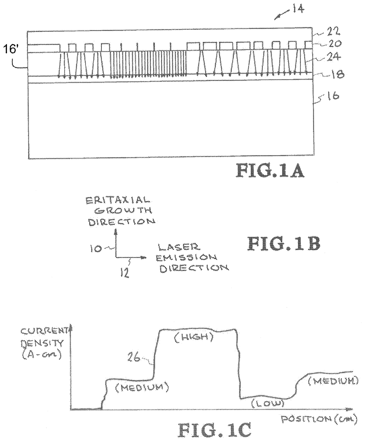
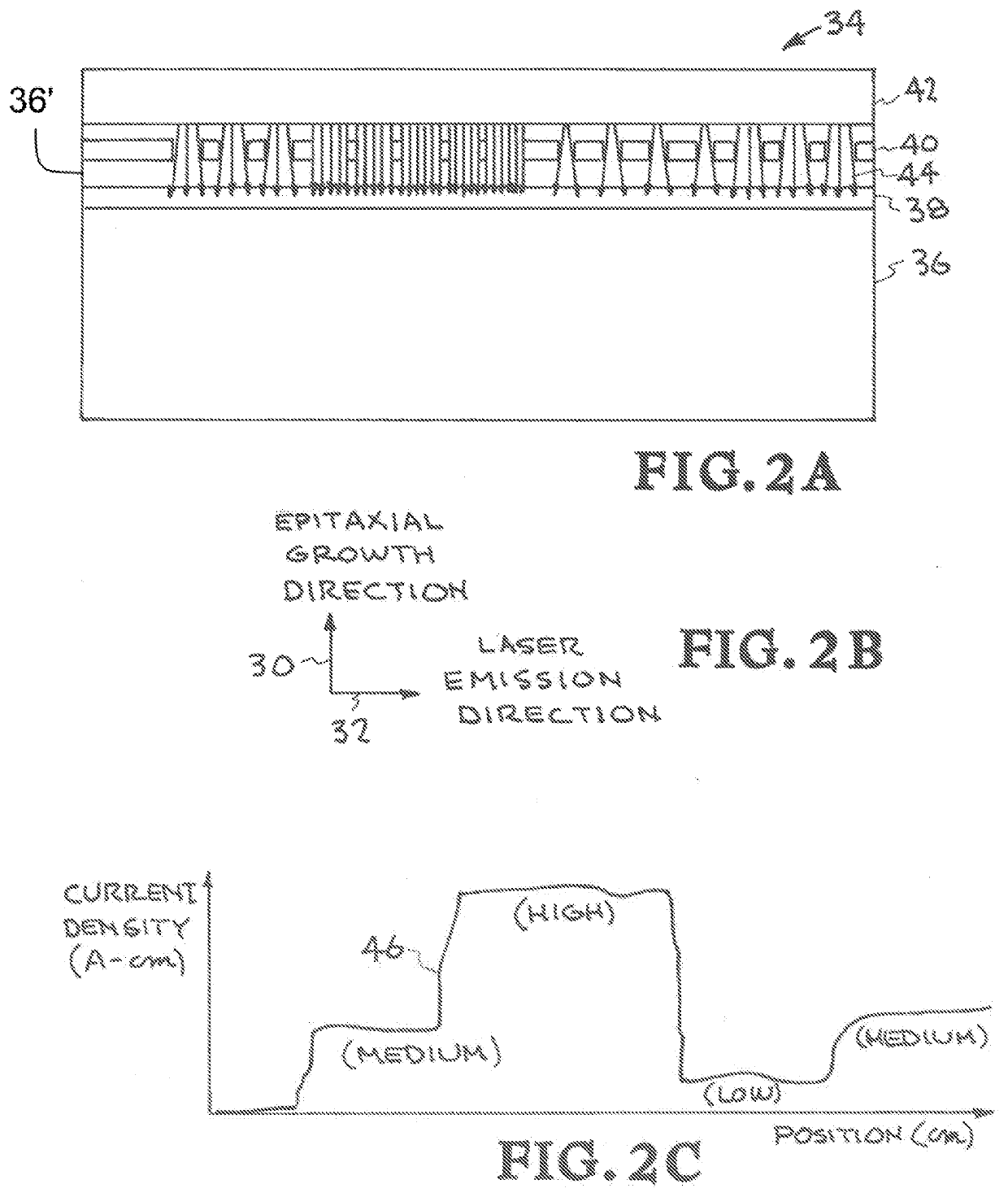
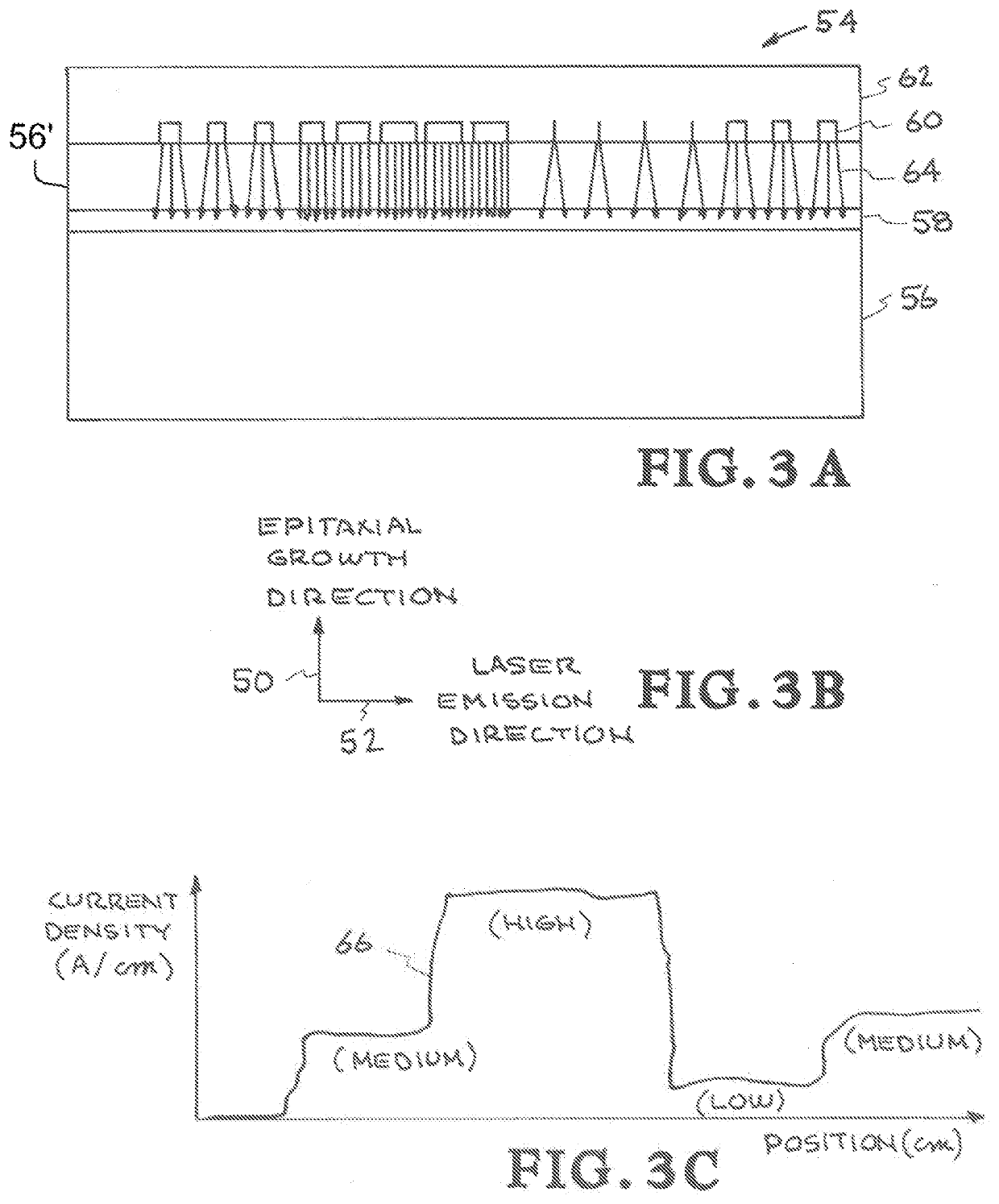
[0018]This technology enables diode lasers which either operate with greater power conversion efficiency or which operate with equivalent power conversion efficiency with greater output power. This is achieved through careful control of the current density profile in the longitudinal direction of the device in order to overcome local current crowding and longitudinal spatial hole burning effects which limit the efficiency and power of long-cavity high power diode lasers.

[0019]Three techniques for controlling the longitudinal current density at the quantum wells along the length of the diode are described. The first is based on high power broad area diode lasers which use a plurality of apertures (also referred to herein as a plurality of vias) through a dielectric to define the emitting area. The second is based on similar devices which instead create the current aperture through proton implantation in the region of semiconductor which is to be rendered non-conductive. In both cases...


PUM

PropertyMeasurementUnit
diameteraaaaaaaaaa
diameteraaaaaaaaaa
current diffusion lengthaaaaaaaaaa

Abstract

The present technology can be used to control the current injection profile in the longitudinal direction of a high-power diode laser in order to optimize current densities as a function of position in the cavity to promote higher reliable output power and increase the electrical to optical conversion efficiency of the device beyond the level which can be achieved without application of this technique. This approach can be utilized, e.g., in the fabrication of semiconductor laser chips to improve the output power and wall plug efficiency for applications requiring improved performance operation.

Description

CROSS-REFERENCE TO RELATED APPLICATIONS[0001]This application claims the benefit of U.S. Provisional Patent Application No. 62 / 648,286 titled “High Power Diode Laser with Engineered Current Density Profile” filed Mar. 26, 2018, incorporated herein by reference.STATEMENT AS TO RIGHTS TO INVENTIONS MADE UNDER FEDERALLY SPONSORED RESEARCH OR DEVELOPMENT[0002]The United States Government has rights in this invention pursuant to Contract No. DE-AC52-07NA27344 between the United States Department of Energy and Lawrence Livermore National Security, LLC, for the operation of Lawrence Livermore National Laboratory.BACKGROUNDField[0003]The present technology relates to semiconductor lasers, and more specifically, it relates to scaling of power and brightness produced by high power semiconductor lasers while maintaining high efficiency operation.Description of Related Art[0004]Significant gains in diode laser brightness over the past decade have been made through lengthening of the laser reson...

Claims


Application Information

Patent Timeline
Patent Type & Authority Applications(United States)
IPC IPC(8): H01S5/042H01S5/343
CPCH01S5/0421H01S5/343H01S5/04254H01S5/16H01S5/168H01S5/1039H01S5/2036H01S5/042
Inventor LEISHER, PAUL O.DERI, ROBERT J.PATRA, SUSANT K.
Owner LAWRENCE LIVERMORE NAT SECURITY LLC
Why Eureka
Try Eureka