Electroluminescent component and display device
- Summary
- Abstract
- Description
- Claims
- Application Information
AI Technical Summary
Benefits of technology
Problems solved by technology
Method used
Image

Examples
embodiment 1
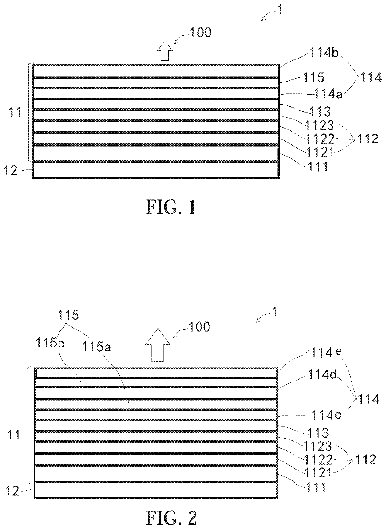
[0034]Referring to FIG. 1, an electroluminescent component 11 of the present disclosure comprises a light output side 100, a first electrode 111, an organic light emitting structure layer 112, a second electrode 113, at least two optical coupling layers 114, and a metal layer 115.
[0035]The first electrode 111 is an anode which is a reflective electrode, is disposed far away from the light output side 100. The first electrode 111 is a laminated structure of indium tin oxide / silver / indium tin oxide (ITO / Ag / ITO).
[0036]The organic light emitting structure layer 112 is disposed on the first electrode 111. The organic light emitting structure layer 112 comprises a hole transport layer 1121, a luminescent layer 1122, an electron transport layer 1123. The hole transport layer 1121 is deposited on the first electrode 111 by a vacuum evaporation. The hole transport layer 1121 has a thickness ranging from 40 nm to 150 nm, and the material of the hole transport layer is at least one of 4,4′,4″-...
embodiment 2
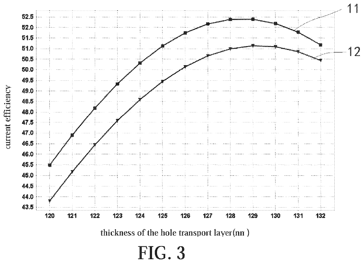
[0044]As shown in FIG. 2, the difference between the electroluminescent component 11 of this embodiment and that of Embodiment 1 is that there are three optical coupling layers 114 and two metal layers 115.
[0045]The three optical coupling layers 114 include a third optical coupling layer 114c, a fourth optical coupling layer 114d, and a fifth optical coupling layer 114e. The metal layers 115 comprise a first metal layer 115a and a second metal layer 115b. Specifically, the third optical coupling layer 114c is disposed on the second electrode 113, the first metal layer 115a is disposed on the third optical coupling layer 114c, the fourth optical coupling layer 114d is disposed on the first metal layer 115a, the second metal layer 115b is disposed on the fourth optical coupling layer 114, and the fifth optical coupling layer 114e is disposed on the second metal layer 115b.
[0046]For increasing the luminous efficiency of the light, in this embodiment, the first metal layer 115a and the...
PUM
 Abstract
Description
Claims
Application Information
 - R&D
- Intellectual Property
- Life Sciences
- Materials
- Tech Scout
- Unparalleled Data Quality
- Higher Quality Content
- 60% Fewer Hallucinations
Browse by: Latest US Patents, China's latest patents, Technical Efficacy Thesaurus, Application Domain, Technology Topic, Popular Technical Reports.
© 2025 PatSnap. All rights reserved.Legal|Privacy policy|Modern Slavery Act Transparency Statement|Sitemap|About US| Contact US: help@patsnap.com