Exposure device
a technology of exposure device and exposure chamber, which is applied in the direction of microlithography exposure apparatus, photomechanical treatment, instruments, etc., can solve the problems of reducing the efficiency of exposure processing, requiring a long period of time, and reducing the accuracy of exposure processing, so as to reduce the volume of the effect of reducing the oxygen concentration in the processing space 20s and shortening the tim
- Summary
- Abstract
- Description
- Claims
- Application Information
AI Technical Summary
Benefits of technology
Problems solved by technology
Method used
Image
Examples
first embodiment
[A] First Embodiment
[1] Configuration of Exposure Device
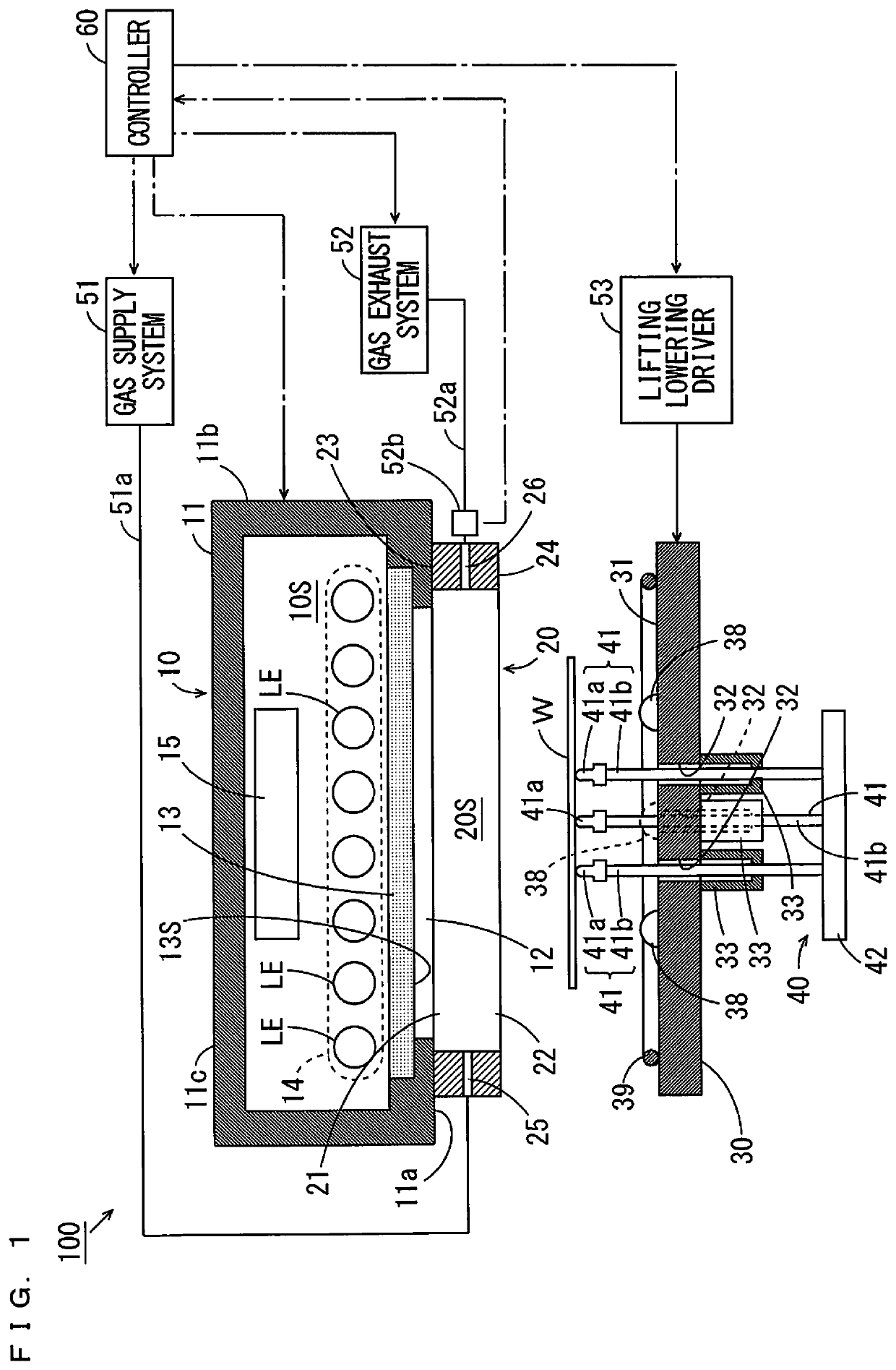
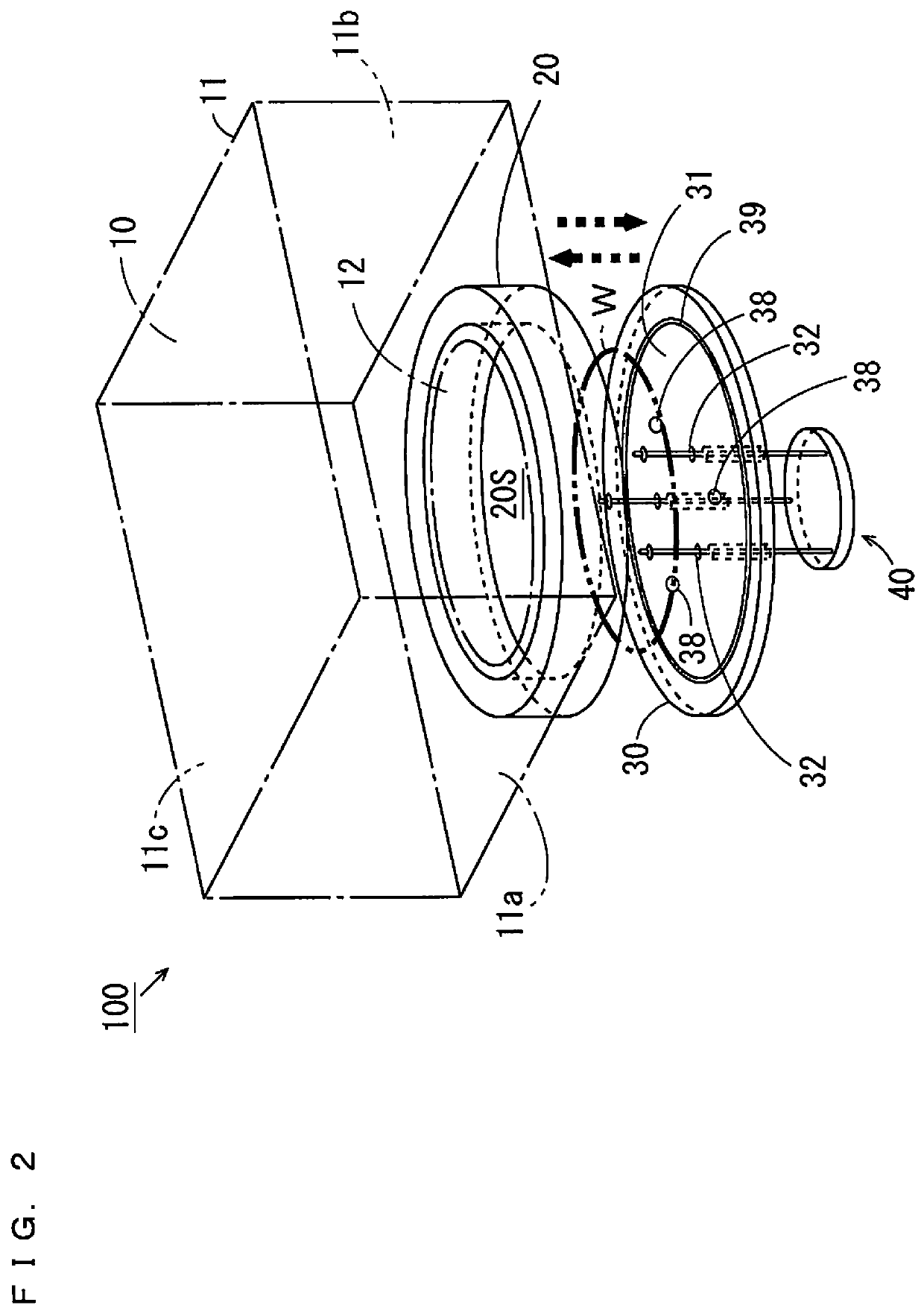
[0068]FIG. 1 is a schematic cross sectional view showing the configuration of an exposure device according a first embodiment, and FIG. 2 is a perspective view for explaining the operation of part of the constituent elements of the exposure device 100 of FIG. 1. As shown in FIG. 1, the exposure device 100 includes a light emitter 10, a peripheral wall member 20, a lower lid member 30, a substrate supporting mechanism 40, a gas supply system 51, a gas exhaust system 52, a lifting lowering driver 53 and a controller 60.
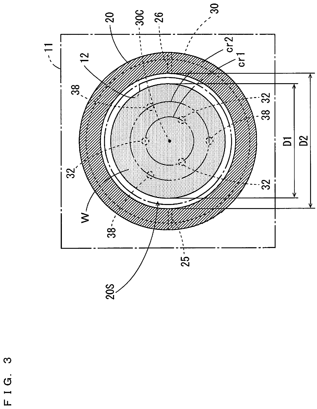
[0069]In the exposure device 100, a processing space 20S in which exposure processing is performed on the substrate W is formed by the peripheral wall member 20. Specifically, the peripheral wall member 20 has a flat cylindrical shape. The space surrounded by an inner peripheral surface of the peripheral wall member 20 is used as the processing space 20S. Further, the peripheral wall member 20 has an upper end surf...
second embodiment
[B] Second Embodiment
[1] Configuration of Exposure Device
[0164]FIG. 17 is a schematic cross sectional view showing the configuration of an exposure device according to a second embodiment of the present invention, and FIG. 18 is a perspective view for explaining the operation of part of the constituent elements of the exposure device 100 of FIG. 17. The configuration and operation of the exposure device 100 of FIGS. 17 and 18 are similar to those of the exposure device 100 of FIGS. 1 and 2 except for the configuration of a peripheral wall member 20.
[2] Configuration of Peripheral Wall Member 20
[0165]FIG. 19 is a schematic plan view of the peripheral wall member 20 of FIG. 17. FIG. 20 is an enlarged perspective view showing the configuration of a first gas flow path 25 of FIG. 19. The peripheral wall member 20 of FIGS. 17, 18 and 19 are different from the peripheral wall member 20 of FIGS. 1, 2 and 3 in the following points.
[0166]As shown in FIGS. 17, 18 and 19, the first gas flow pa...
PUM
| Property | Measurement | Unit |
|---|---|---|
| wavelength | aaaaa | aaaaa |
| wavelength | aaaaa | aaaaa |
| inner diameter D2 | aaaaa | aaaaa |
Abstract
Description
Claims
Application Information


