

Display panel, manufacturing method thereof, and display device
a technology of display panel and manufacturing method, applied in non-linear optics, instruments, optics, etc., can solve problems such as affecting appearance, and achieve the effects of reducing the contact impedance of side bonding, increasing the space for side filler coating, and increasing the cross-sectional area of bonding lead
- Summary
- Abstract
- Description
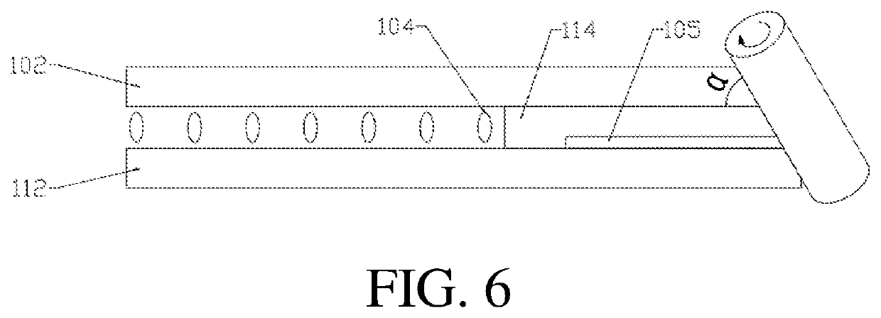
- Claims
- Application Information
AI Technical Summary
Benefits of technology
Problems solved by technology
Method used
Image

Examples
Embodiment Construction
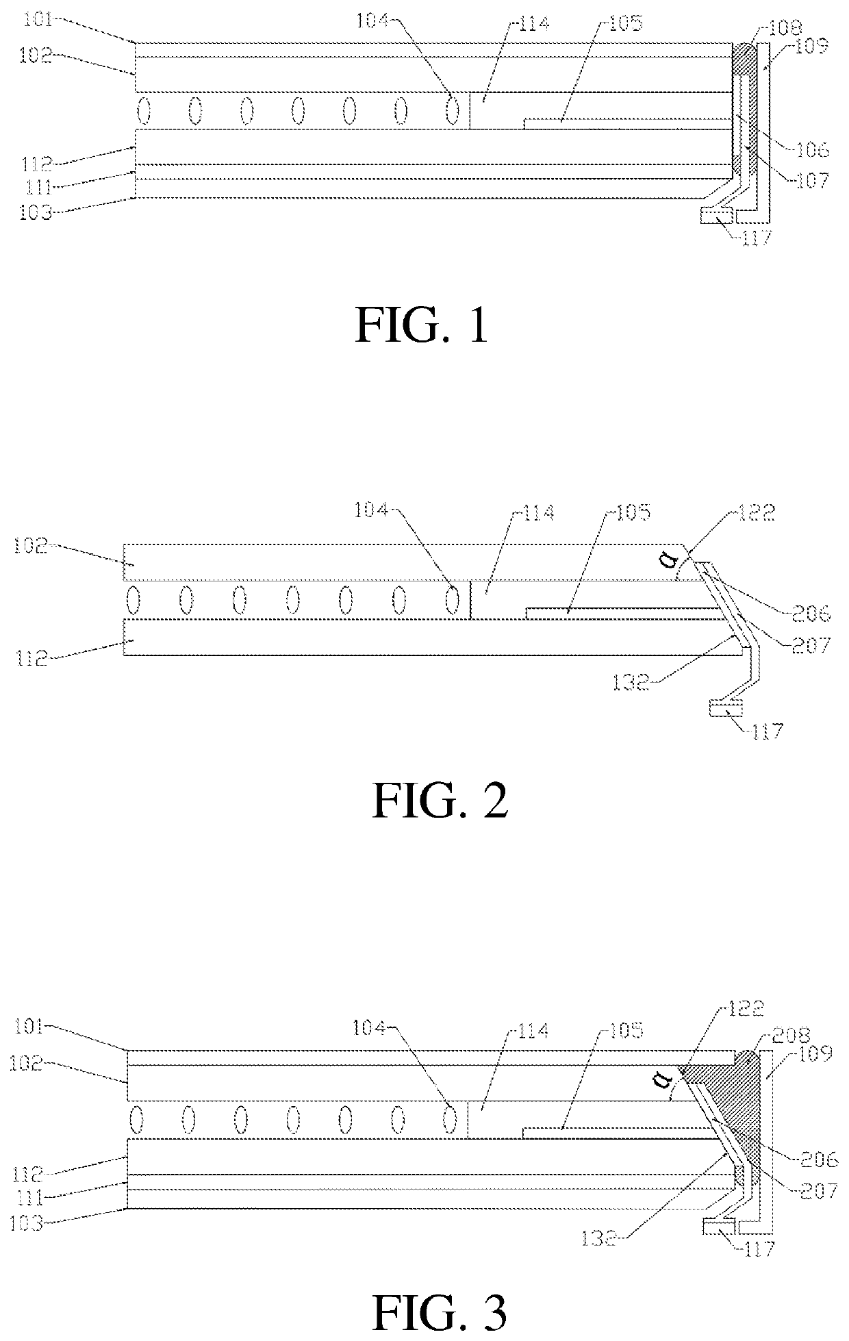
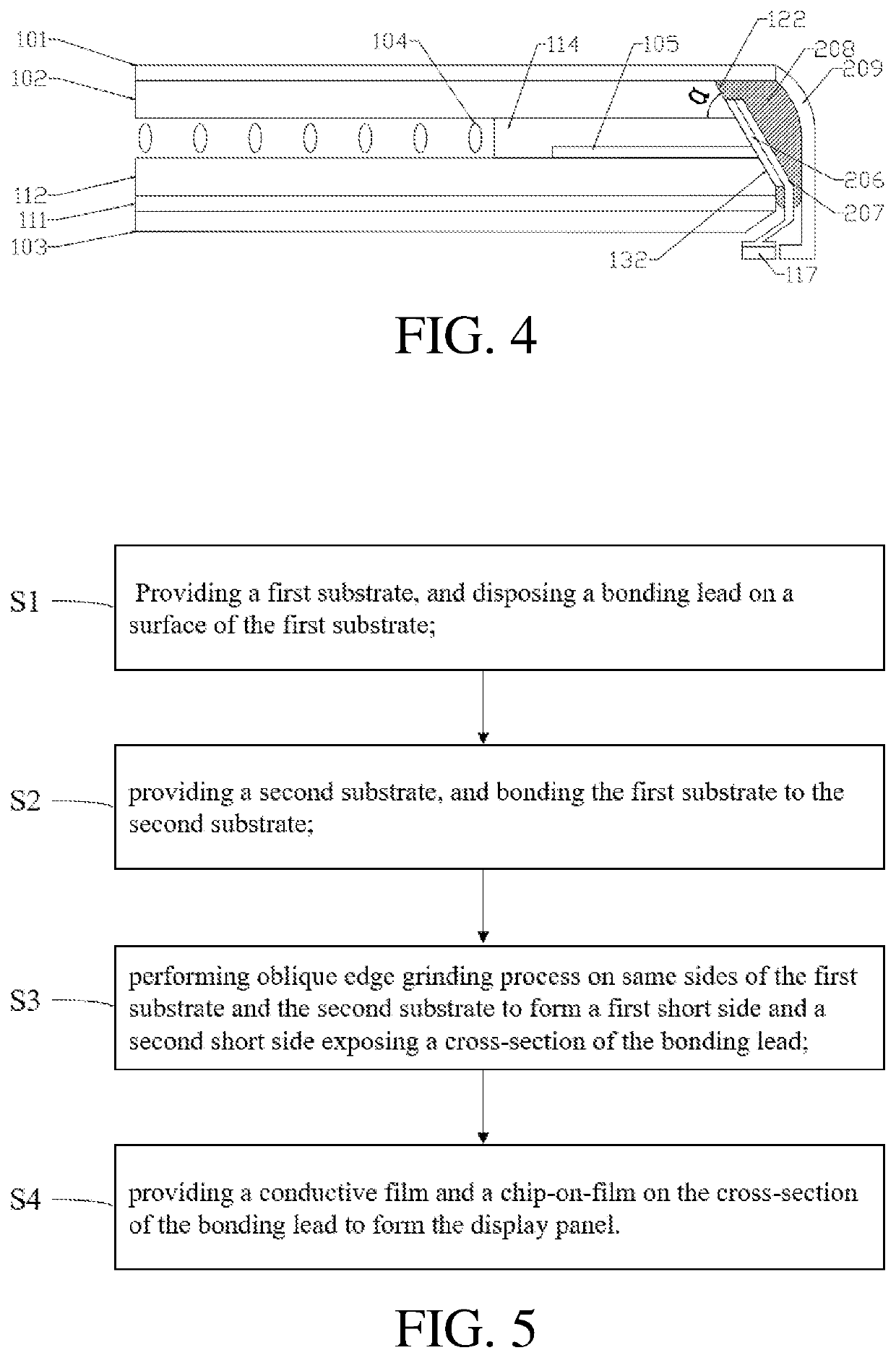
technical solutions in the embodiments of the present invention are clearly and completely described in the following with reference to the accompanying drawings in the embodiments of the present invention. It is obvious that the described embodiments are only a part of the embodiments of the invention, and not all of the embodiments. All other embodiments obtained by a person skilled in the art based on the embodiments of the present invention without creative efforts are within the scope of the present invention.
[0039]In the description of the present invention, it is to be understood that the terms “center”, “longitudinal”, “transverse”, “length”, “width”, “thickness”, “upper”, “lower”, “front”, “back”, “left”, “right”, “vertical”, “horizontal”, “top”, “bottom”, “inside”, “outside”, etc. is based on the orientational or positional relationship shown in the drawings. It is merely for the convenience of describing the present invention and simplifying the description, instead of in...
PUM
| Property | Measurement | Unit |
|---|---|---|
| angle | aaaaa | aaaaa |
| inclination angle | aaaaa | aaaaa |
| angle | aaaaa | aaaaa |
Abstract
Description
Claims
Application Information