Connection structure between dielectric waveguide line and waveguide

a dielectric waveguide and connection structure technology, applied in the direction of waveguides, electrical devices, coupling devices, etc., can solve the problems of difficult to employ ltcc in the sub-terahertz band, low dimensional accuracy of ltcc, and low loss of ltcc, etc., to achieve satisfactory transmission characteristics

Active Publication Date: 2021-04-22
NEC CORP
View PDF0 Cites 0 Cited by
  • Summary
  • Abstract
  • Description
  • Claims
  • Application Information

AI Technical Summary

Benefits of technology

[0014]According to the present disclosure, in the connection structure between the dielectric waveguide line and the waveguide, by forming a local recess in the dielectric substrate without thinning the entire dielectric substrate, satisfactory transmission characteristics can be achieved while ensuring mechanical strength of the dielectric substrate.

Problems solved by technology

Since the dimensional accuracy of LTCC, which is commonly used in the millimeter wave band, is not very high and the loss thereof is relatively large, it is difficult to employ LTCC in the sub-terahertz band.
On the other hand, although the loss of the resin substrate is low, the resin substrate has low rigidity, the methods of mounting the resin substrate are limited, and its dimensional accuracy is not very high, which makes it difficult to employ the resin substrate in the sub-terahertz band, like the LTCC.
However, since the formation of via holes is difficult, the use of the via holes has been limited, and thus the via holes have not been widely used.

Method used


Image

  • Connection structure between dielectric waveguide line and waveguide
  • Connection structure between dielectric waveguide line and waveguide
  • Connection structure between dielectric waveguide line and waveguide

Examples


first example embodiment

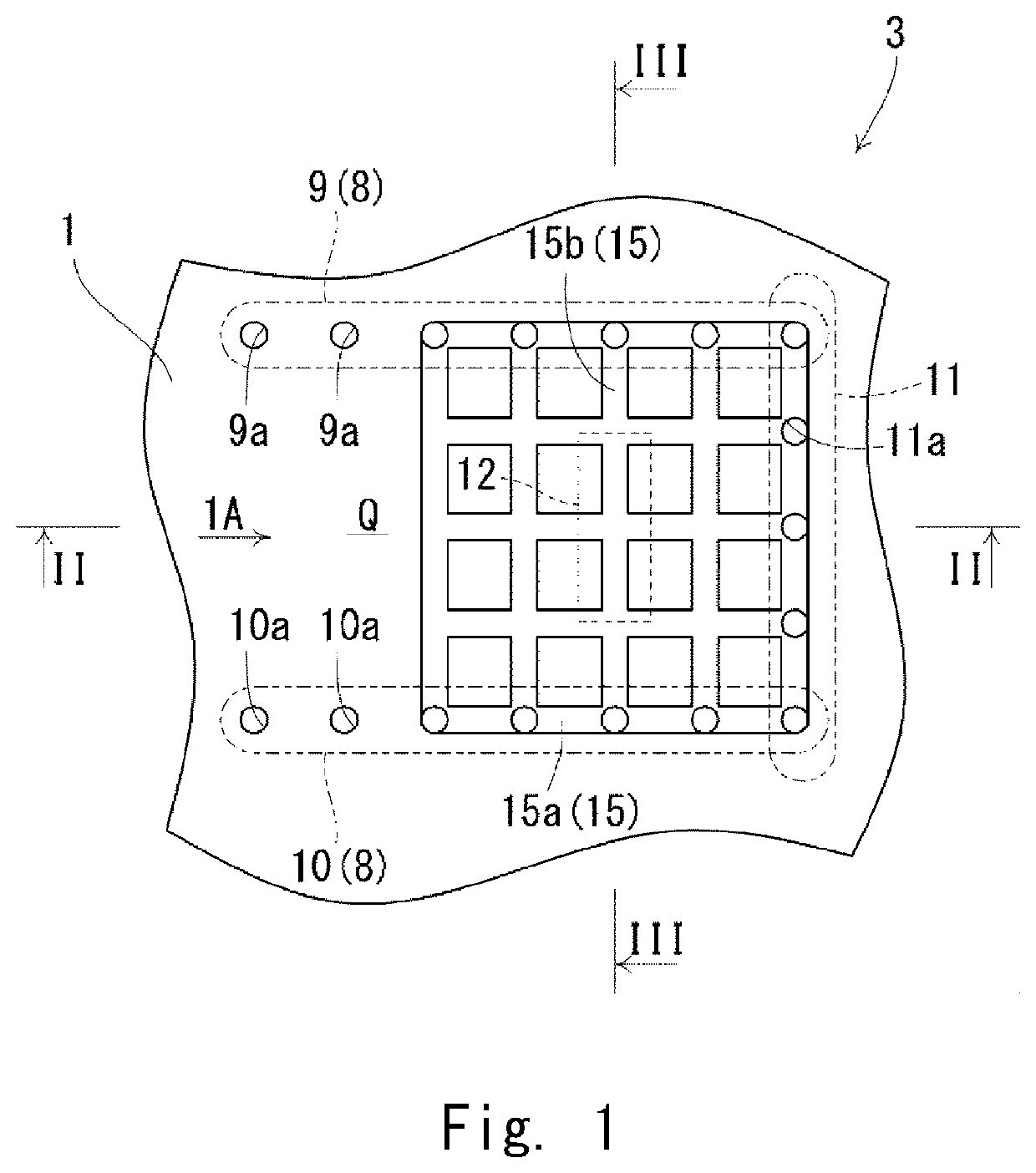
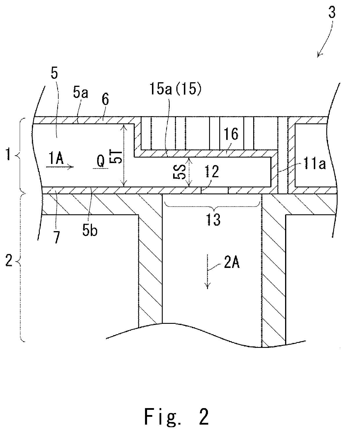
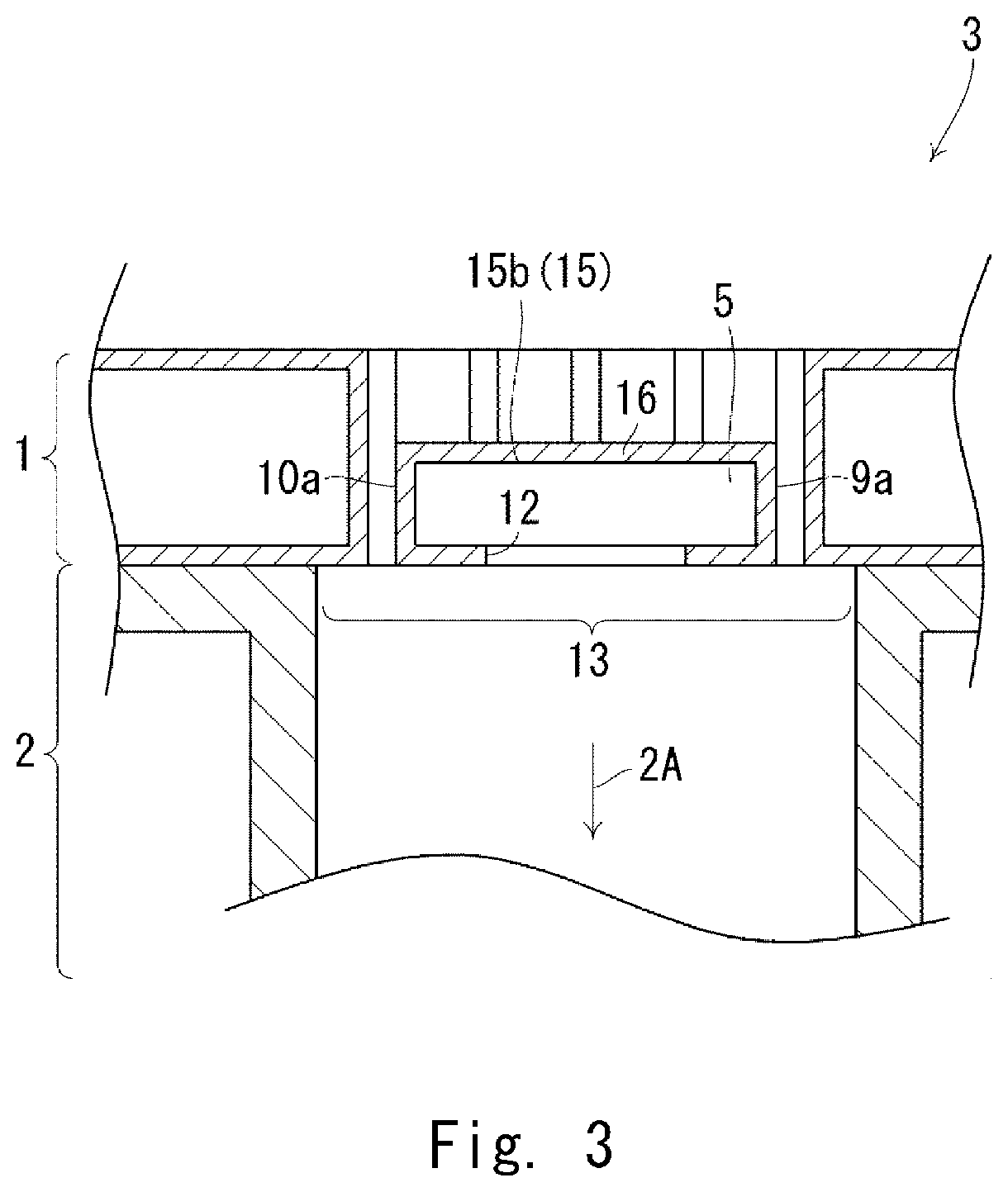
[0026]Hereinafter, a first example embodiment will be described with reference to FIGS. 1 to 3. FIG. 1 is a plan view of a connection structure according to the first example embodiment. FIG. 2 is a cross-sectional view taken along the line II-II of FIG. 1. FIG. 3 is a cross-sectional view taken along the line of FIG. 1.

[0027]FIGS. 1 to 3 show a connection structure 3 between a dielectric waveguide line 1 and a rectangular waveguide 2. As shown in FIG. 2, the connection structure 3 includes a dielectric waveguide line 1 and a rectangular waveguide 2. The dielectric waveguide line 1 and the rectangular waveguide 2 are connected to each other in such a way that a transmission direction 1A of an operating frequency signal in the dielectric waveguide line 1 becomes orthogonal to a transmission direction 2A of a operating frequency signal in the rectangular waveguide 2. The operating frequency signal is a specific example of a high frequency signal.

[0028]As shown in FIGS. 1 and 2, the di...

second example embodiment

[0055]Next, a second example embodiment will be described with reference to FIG. 4. Hereinafter, a difference between this example embodiment and the first example embodiment will be mainly described, and the repeated description will be omitted.

[0056]As shown in FIG. 4, in this example embodiment, the plurality of recesses 15 do not include the plurality of transmission-direction translational recesses 15a, and instead include only the plurality of transmission-direction orthogonal recesses 15b. The plurality of transmission-direction orthogonal recesses 15b are formed in the vicinity of the coupling window 12. Thus, the area where the plurality of recesses 15 are formed is smaller as compared with the first example embodiment, and thus the uniformity of the function as the upper surface of the waveguide is deteriorated, but productivity and mechanical strength can be improved.

third example embodiment

[0057]Next, a third example embodiment will be described with reference to FIG. 5. Hereinafter, a difference between this example embodiment and the first example embodiment will be mainly described, and the repeated description will be omitted.

[0058]As shown in FIG. 5, in this example embodiment, the plurality of recesses 15 do not include the plurality of transmission-direction orthogonal recesses 15b, and instead include only the plurality of transmission-direction translational recesses 15a. The plurality of transmission-direction translational recesses 15a are formed in the vicinity of the coupling window 12. Thus, the area where the plurality of recesses 15 are formed is smaller as compared with the first example embodiment, and thus the uniformity of the function as the upper surface of the waveguide is deteriorated, but productivity and mechanical strength can be improved.


PUM

PropertyMeasurementUnit
frequencyaaaaaaaaaa
thicknessaaaaaaaaaa
thicknessaaaaaaaaaa

Abstract

A connection structure includes a dielectric waveguide line and a rectangular waveguide. The dielectric waveguide line transmits a high-frequency signal in a transmission region surrounded by a first conductor layer, a second conductor layer, and two arrays of via hole groups. A coupling window is formed in the second conductor layer. The rectangular waveguide is disposed in such a way that an open end surface of the rectangular waveguide faces the coupling window, and that the transmission direction of the dielectric waveguide line becomes orthogonal to the transmission direction of the rectangular waveguide. A plurality of recesses are formed on a first substrate surface in the vicinity of the coupling window. A recessed conductor layer electrically connected to the first conductor layer is formed on inner wall surfaces of the plurality of recesses.

Description

TECHNICAL FIELD[0001]The present disclosure relates to a connection structure between a dielectric waveguide line and a waveguide.BACKGROUND ART[0002]Recently, communication traffic has increased rapidly due to the expansion of large-capacity communication applications such as streaming video in addition to the increase in the number of terminals because of the spread of mobile terminal devices such as smartphones. Under such circumstances, it is expected to achieve large-capacity communication using the sub-terahertz band having a wide frequency band. The sub-terahertz band here generally refers to a frequency band of 100 GHz or more.[0003]In a high frequency band module such as a millimeter wave band according to related art, LTCC (Low Temperature Co-fired Ceramics), which is easy to be multilayered and has a high degree of freedom in design, is widely used. Resin substrates are often used, because the loss of the material is inherently low and transmission loss of the resin subst...

Claims


Application Information

Patent Timeline
Patent Type & Authority Applications(United States)
IPC IPC(8): H01P5/08H01P3/02H01P3/08H01P3/12H01P3/16
CPCH01P5/08H01P3/026H01P3/16H01P3/12H01P3/08H01P5/107H01P3/121H01P5/024
Inventor ITO, MASAHARU
Owner NEC CORP
Why Eureka
Try Eureka