Packaged environmental sensor

a sensor and environmental technology, applied in the direction of fluid speed measurement, instruments, forming microstructure systems, etc., can solve the problems of environmental sensors being exposed to aggressive agents, task is rendered problematic, and solution, however, presents limits

Active Publication Date: 2021-06-03
STMICROELECTRONICS SRL
View PDF6 Cites 0 Cited by
  • Summary
  • Abstract
  • Description
  • Claims
  • Application Information

AI Technical Summary

Benefits of technology

[0035]The packaged environmental sensor described affords several advantages. In the first place, the control chip, which is located on the opposite side of the supporting structure with respect to the sensor die, is enclosed in a space that, in use, may be conveniently sealed with the gasket between the collar and the margin of the opening in the casing of the electronic device, where the packaged environmental sensor is installed. Consequently, the packaged environmental sensor is never exposed to the physically and / or chemically aggressive external environment. Therefore, not only is the control circuit in intrinsically safer conditions as compared to known environmental sensors, but there is also greater freedom of choice of the protective material in which the control circuit is embedded. Furthermore, the control chip is isolated from the external light so as to remain immune therefrom even though its surface may be sensitive to light.

Problems solved by technology

Also in the case of devices commonly used as wearable devices, in fact, environmental sensors may be exposed to aggressive agents, for example chlorine in the water of a swimming pool, seawater, mineral oils or substances present on the skin, such as sweat or some perfumes.
If, for the sensor die and for the control device, an acceptable level of protection can frequently be obtained with just the gel, there, however, arises the problem of sealing also the device in which the environmental sensor is incorporated.
The task is rendered problematical by the packaging structures of known environmental sensors.
The solution, however, presents limits both because the lid is complex and costly to produce and on account of the problems that arise during the soldering step.
The result is a substantial risk of failure or weakening of the connection between the lid and the supporting structure.

Method used


Image

  • Packaged environmental sensor
  • Packaged environmental sensor
  • Packaged environmental sensor

Examples


Embodiment Construction

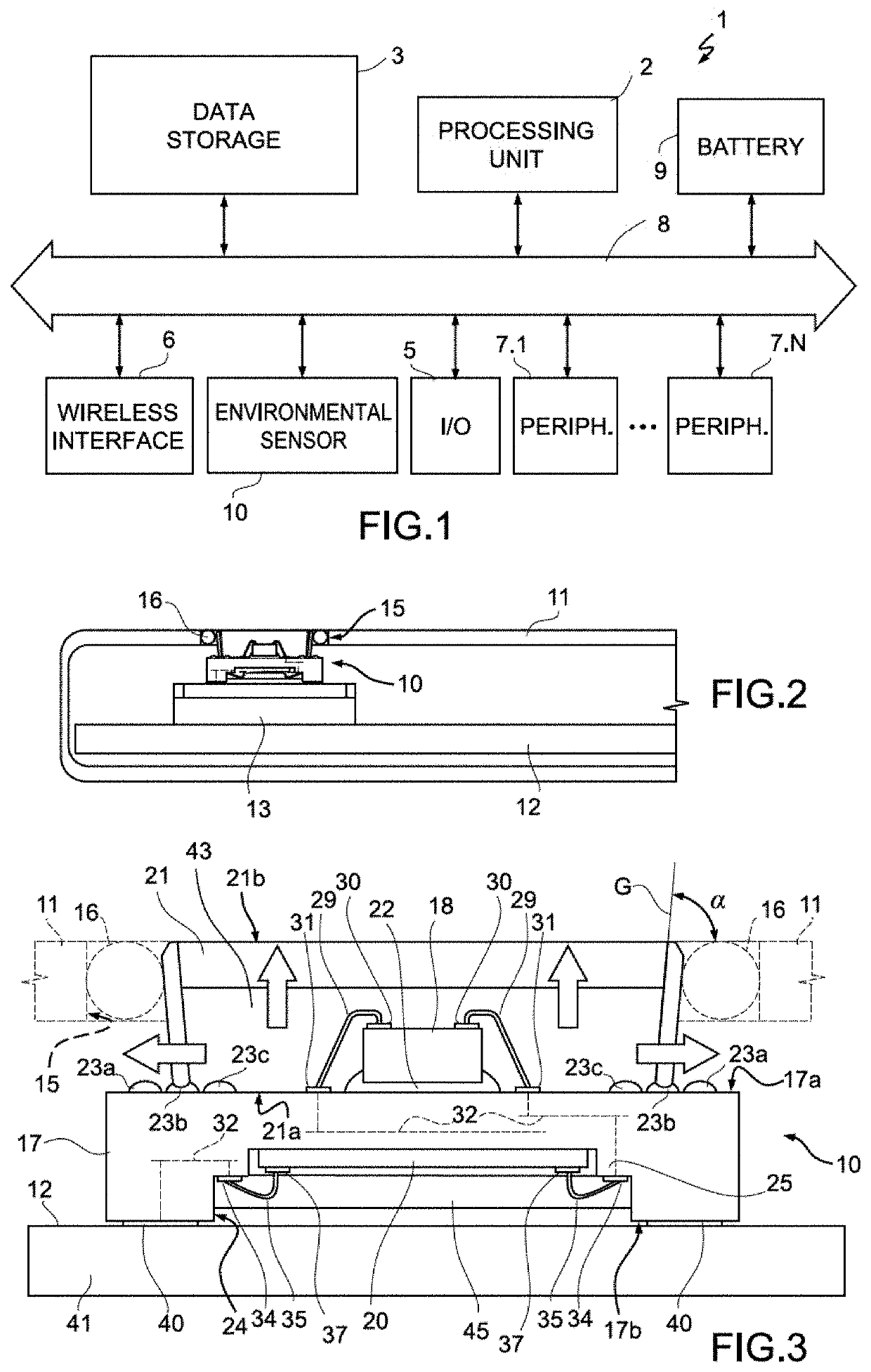
[0016]With reference to FIG. 1, an electronic device is designated as a whole by the reference number 1 and may be an electronic device of any type, in particular, but not exclusively, a wearable device, such as a watch, a bracelet, or a smart band, a computer, such as a mainframe, a personal computer, a laptop, or a tablet, a smartphone, a digital musical player, a digital camera, or any other device adapted to process, store, transmit, or receive information. The electronic device 1 may be a general-purpose computer system or may be embedded in a device, an apparatus, or a further system.

[0017]The electronic device 1 comprises a processing unit 2, data-storage media 3, and a packaged environmental sensor 10, and may moreover be provided with an input / output (I / O) device 5 (for example a keypad, a mouse, or a touchscreen), a wireless interface 6, peripherals 7.1, . . . , 7.N, and possibly further auxiliary devices, here not illustrated. The components of the electronic device 1 may...


PUM


Abstract

A packaged environmental sensor includes a supporting structure and a sensor die, which incorporates an environmental sensor and is arranged on a first side of the supporting structure. A control chip is coupled to the sensor die and is arranged on a second side of the supporting structure opposite to the first side. A lid is bonded to the first side of the supporting structure and is open towards the outside in a direction opposite to the supporting structure. The sensor die is housed within the lid.

Description

BACKGROUNDTechnical Field[0001]The present disclosure relates to a packaged environmental sensor.Description of the Related Art[0002]As is known, environmental sensors are sensors that enable detection of magnitudes of the external environment, such as pressure or humidity. The fields of use of environmental sensors are extremely varied. Among other applications, there has recently been a widespread use of environmental sensors in so-called wearable devices, such as watches, bracelets, and smartbands, which also enable detection of body parameters.[0003]An environmental sensor normally comprises a sensor die, for example of a MEMS (MicroElectroMechanical System) type, and a control circuit, integrated in a separate control chip, also referred to as ASIC (Application-Specific Integrated Circuit) chip. The sensor die and the control chip are enclosed within a packaging structure (normally referred to as package), which comprises a supporting structure, normally of ceramic, and a lid. ...

Claims


Application Information

Patent Timeline
Patent Type & Authority Applications(United States)
IPC IPC(8): B81B7/00
CPCB81B7/0058B81B2207/012B81B2201/0264B81B2207/092B81B2201/0292B81B2207/07B81B2201/0278B81B7/02B81B2201/02B81B7/0061B81C1/0023B81C2203/0792B81C2203/0145
Inventor GHIDONI, MARCO OMAR
Owner STMICROELECTRONICS SRL
Why Eureka
Try Eureka