Dipole element for superconducting circuits

a dipole element and superconducting technology, applied in the field of superconducting dipole elements, can solve the problems of system instability, limiting the dynamic range of engineered process or deformation of quantum states, and affecting the performance of superconducting magnets/coils, so as to improve the ability of parametric pumping

a dipole element and superconducting technology, applied in the field of superconducting dipole elements, can solve the problems of system instability, limiting the dynamic range of engineered process or deformation of quantum states, and affecting the performance of superconducting magnets/coils, so as to improve the ability of parametric pumping

US20210234086A1Active Publication Date: 2021-07-29UNIVERSITÉ PARIS CITÉ +5

Image

  • Dipole element for superconducting circuits
  • Dipole element for superconducting circuits

Examples


Embodiment Construction

lass="d_n">[0032]It is well understood that the embodiments which will be described hereinafter are in no way limitative. Variants of the invention can be considered comprising only a selection of the characteristics described hereinafter, in isolation from the other characteristics described, if this selection of characteristics is sufficient to confer a technical advantage or to differentiate the invention with respect to the state of the prior art. This selection comprises at least one, preferably functional, characteristic without structural details, or with only a part of the structural details if this part alone is sufficient to confer a technical advantage or to differentiate the invention with respect to the state of the prior art.

[0033]In particular, all the variants and all the embodiments described can be combined together if there is no objection to this combination from a technical point of view.

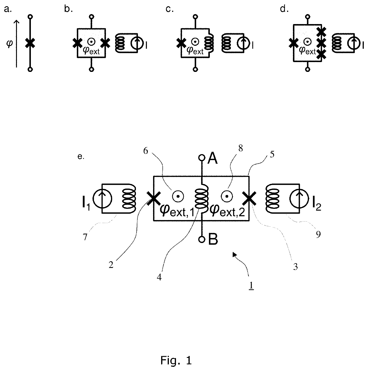
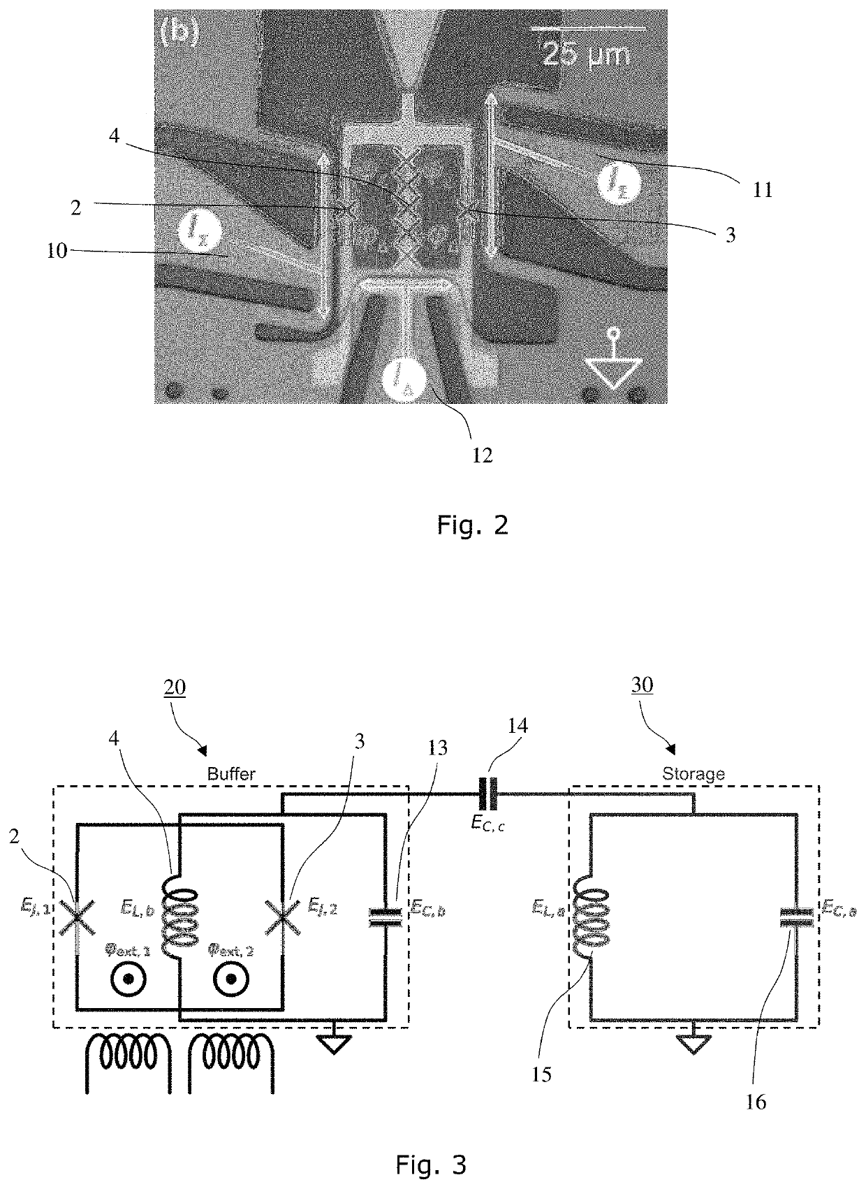
[0034]In the Figures, the elements that are common to several Figures keep ...


PUM

PropertyMeasurementUnit
inductanceaaaaaaaaaa
superconductingaaaaaaaaaa
magnetic fluxaaaaaaaaaa

Abstract

The present invention relates to an inductive dipole element for a superconducting microwave quantum circuit. The dipole element comprises a DC-SQUID formed by a pair of Josephson junctions shunted by an inductance, wherein the Josephson junctions have equal energy, and the Josephson junctions and the inductance are arranged such that each of the junctions forms a loop with the inductance. The two loops are asymmetrically threaded with external magnetic DC fluxes φext1 and φext2, respectively, such that φext1=π and φext2=0, wherein parametric pumping is enabled by modulating the total flux φΣ=φext,1+φext,2 threading the dipole element, thereby allowing even-wave mixing between modes that participate in the dipole element with no Kerr-like interactions.

Description

FIELD OF THE INVENTION[0001]The present invention relates generally to a non-linear mixing element for superconducting microwave quantum circuits. More particularly, the present invention relates to a superconducting dipole element for use in a superconducting microwave quantum circuit.[0002]The field of the invention is more particularly, but non-limitatively, that of superconducting circuit based quantum technologies.BACKGROUND OF THE INVENTION[0003]Electromagnetic radiation waves do not normally interact with each other as they travel in simple media such as vacuum or air. To have two or more waves interact, they should encounter some non-linearity.[0004]For example, in the field of non-linear optics, one uses specific crystals to double the frequency of an incoming radiation via a process called second harmonic generation. This conversion arises from the slightly non-linear potential energy that the electrons experience in the crystal leveraged by the large electromagnetic field...

Claims


Application Information

Patent Timeline
29 Jul 2021
Publication
US20210234086A1
IPC
H01L39/22; H01L39/02; H03K19/195; H01F6/06; H01B12/02; G01R33/035; G06N10/00; H10N60/80
CPC
H01L39/223; H01L39/025; H03K19/1954; G06N10/00; H01B12/02; G01R33/0358; H01F6/06; G01R33/0354
Inventors
LESCANNE, RAPHAËL; LEGHTAS, ZAKI